Chapter 2
Packaging, Memory & the Server
A finished chip is helpless on its own — it needs a body to plug into the world, a fast workspace to hold numbers while it computes, and hundreds of supporting parts around it before it becomes a machine that can actually run AI.
Packaging — Giving the Die a Body
Go back to where Chapter 1 left off. A wafer — a thin, round disc of silicon about the size of a large dinner plate — comes out of the fab with hundreds of chips etched into its surface, each one still attached to its neighbors like cookies on a sheet. Each individual chip, before it's cut free, is called a die. On its own, a die is useless. It has no legs, no pins, no way to send or receive electricity, and it's so thin and brittle that touching it with a bare finger could crack it. Packaging is the process of taking that raw, fragile die and giving it a body: something that protects it, something that lets it plug into the outside world, and something a human — or a robot — can actually pick up and place onto a circuit board.
For decades, packaging was almost an afterthought. The hard part was making the chip; wrapping it up was routine. The classic method, called wire bonding, is exactly what it sounds like: hair-thin gold or copper wires are soldered from tiny metal pads on the edge of the die out to the pins of a protective casing, a little like running individual telephone wires from a rooftop antenna down to the house. It's cheap, it's mature, and for a single chip doing a single job, it works fine.
AI chips broke that model. An H100 or a Blackwell-generation GPU doesn't work alone — it needs to sit inches away from a stack of ultra-fast memory (more on that in 2.2) and exchange staggering amounts of data with it, thousands of times a second. Wire bonding, with its handful of hair-thin wires strung out to the edge of the chip, simply cannot carry that much data that fast. The bottleneck moved. It used to be "can we make a fast enough transistor?" Increasingly, in AI chips, it became "can we get the finished chip talking to its memory fast enough?" That question is what advanced packaging exists to answer.
CoWoS: Building a Chip Out of Chips
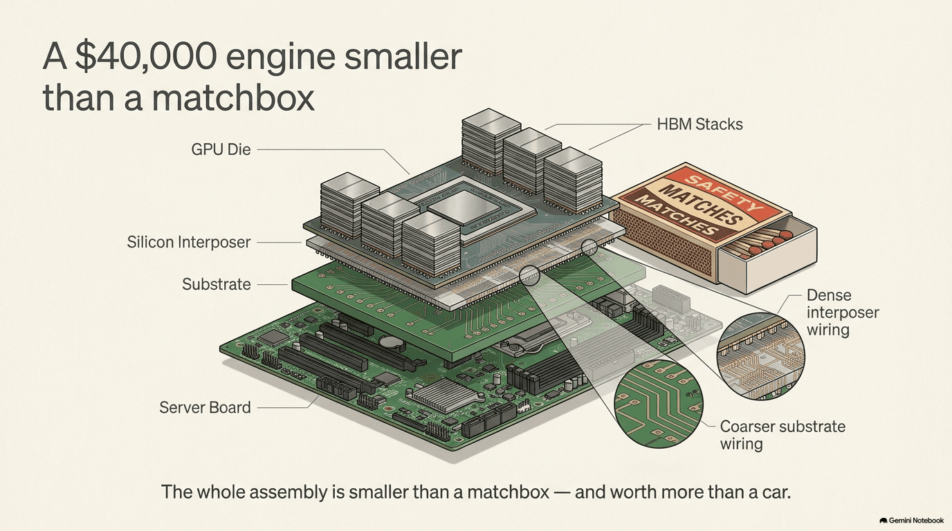
The leading answer, at least for now, is a technique called CoWoS — short for Chip-on-Wafer-on-Substrate. The name is really just a list of the layers, read bottom to top in reverse, and once you see it as a sandwich, the whole idea clicks into place.
Picture three layers stacked on top of each other, like a club sandwich:
- The bottom layer is the substrate — think of it as the foundation slab. It's a small circuit board of its own, and it's what eventually gets soldered down onto the server's motherboard. It carries the electrical connections out to the rest of the machine and physically holds everything up.
- The middle layer is the interposer — a thin, blank slice of silicon, cut from its own wafer, with no transistors of its own. Its only job is wiring. Engraved into its surface are tens of thousands of microscopic copper connections, packed far more densely than anything a normal circuit board could achieve, because it's made with the same precision lithography tools used to make chips (see Chapter 1). Think of the interposer as a miniature multi-lane highway system built specifically to connect two or more chips sitting right next to each other.
- The top layer is the chips themselves — the GPU die and, right beside it, several stacks of high-bandwidth memory (again, more in 2.2). They're placed directly onto the interposer, not wired to it from the side.
Why go through all this trouble? Distance and density. On a normal circuit board, wires connecting one chip to another might be a few millimeters wide and spaced relatively far apart, because a circuit board is made with much coarser tools than a chip fab. That's fine for a chip that only needs to send data occasionally. But a GPU and its memory need to exchange enormous amounts of data continuously, and every extra millimeter of wire, and every drop in connection density, either slows that exchange down or burns more electricity moving the data. By building the "wiring layer" — the interposer — out of silicon itself, using chip-grade tools instead of circuit-board-grade tools, packaging engineers can fit orders of magnitude more connections into the same space, and place the memory close enough to the GPU that the round trip takes almost no time at all. It's the difference between shouting a question across a football field and turning to whisper it to the person standing right next to you.
This is also why packaging became a genuine chokepoint in the AI supply chain — a step where the whole industry funnels through a small number of hands. Etching a silicon interposer with tens of thousands of precise connections, then stacking and bonding chips onto it with near-zero defects, at the volumes AI demands, turns out to be its own extremely hard manufacturing discipline, separate from making the transistors in the first place. Only a small number of factories in the world can currently do it at the scale and yield AI companies need. TSMC — the same company that fabricates the transistors in Chapter 1 — is the dominant name in CoWoS today, which means a chip can be finished at the transistor level and still be stuck waiting in line for its "body" to be built. When people in the industry talk about AI chip shortages, they increasingly mean a packaging shortage, not a transistor shortage.
To relieve that pressure, packaging houses are experimenting with new formats. One approach under development is moving from small round packaging plates to large rectangular panels — essentially building many packages side by side on a bigger sheet at once, the way a printing press gets more copies per run by using a bigger sheet of paper, instead of running the press more times. Another is switching the substrate material from organic resin to glass, which stays flatter and more stable as packages get larger and hotter, though this approach is still years from broad production. Both are attempts to squeeze more packaged chips out of the same factory floor space and time.
The Companies That Build the Body
TSMC does the CoWoS step itself, inside its own factories, immediately after making the chip — which is part of why it has become such a chokepoint; the same company controls both the transistor and the way it gets its body. But a large amount of traditional packaging and final testing work — putting the finished package into its outer casing, testing that every connection works, and shipping it out the door — is handled by specialist companies called OSATs (short for Outsourced Semiconductor Assembly and Test). Amkor is the largest OSAT headquartered in the United States and is building a large new campus in Arizona specifically to sit near TSMC's American fabs. ASE is the largest OSAT in the world overall, based in Taiwan. Neither company designs chips or makes the underlying transistors — their expertise is entirely in the delicate, precise work of turning a bare die into a finished, tested part.
Stacking memory chips on top of each other (the "HBM" towers described in the next section) requires its own specialized tool: a machine that presses each ultra-thin memory die onto the one below it with heat and pressure precise enough not to crack a wafer-thin sliver of silicon, called a thermo-compression bonder. Kulicke & Soffa is one of the few companies that builds these.
Chiplets: Why One Big Chip Became Several Small Ones
There's a second reason advanced packaging matters, beyond connecting a GPU to its memory: it's changing how the "brain" chip itself gets built in the first place.
For most of the industry's history, a chip was one continuous piece of silicon: every transistor on it was etched in a single pass through the fab. That worked fine while chips were small. But as designers wanted to pack in more and more transistors, they ran into a physical wall — the lithography tools that etch a chip (Chapter 1's EUV machines) can only expose a certain maximum area in one shot, called the reticle limit. Push a design past that limit, and you simply cannot print it as one piece.
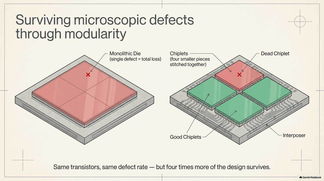
There's also a yield problem. Manufacturing at the nanometer scale is never perfect — a certain number of tiny defects always occur somewhere on a wafer. If a chip is enormous, a single defect anywhere on it ruins the entire, very expensive chip. If instead that same chip is broken into several smaller pieces — each one, say, a quarter of the size — a defect only ruins one small piece, and the other three are still fine. Smaller pieces are dramatically cheaper to throw away when something goes wrong, and dramatically more likely to come out perfect in the first place.
The solution the industry converged on is called chiplets: instead of building one giant chip, build several smaller ones, each optimized for its own job — one might specialize in raw computation, another in moving data around — and then stitch them back together into a single package using exactly the kind of dense, high-speed interposer wiring described above. From the outside, a chiplet-based processor looks and behaves like one chip. Inside, it's a small city of separately manufactured pieces, wired together closely enough that they can act as one. Advanced packaging isn't just what connects a GPU to its memory anymore — it's what lets the "GPU" itself exist as a design at all, at the sizes AI now demands.
The yield math behind this is worth spelling out, because it explains why the industry was willing to take on the added complexity of stitching chips back together rather than simply printing them whole. Imagine a wafer where, on average, one small defect appears somewhere in every square inch. Print one giant chip that covers four square inches, and there's a good chance that single defect lands somewhere inside it — and the entire chip, representing a huge amount of expensive fab time, is scrapped. Print four separate one-square-inch chiplets instead, and that same defect only ruins one of them; the other three ship normally. The larger the design, the more painfully this math bites, which is exactly why the largest, most expensive AI chips were among the first to move to chiplets. The tradeoff is that a chiplet-based design needs its own internal "roads" — the interposer wiring — fast and dense enough that the separate pieces don't feel the seams between them, which is precisely the packaging problem this section opened with.
Memory — The Chip's Workspace
A chip that computes needs somewhere to put the numbers while it's working on them — the same way a person doing long division needs scratch paper, not just a calculator that instantly forgets everything the moment it produces one answer. That scratch paper, in a computer, is called memory, and the most common kind used for it is DRAM (Dynamic Random-Access Memory).
DRAM stores each bit of data — each 1 or 0 — as a tiny electrical charge sitting in a microscopic capacitor, a component that holds a small amount of charge the way a tiny bucket holds a small amount of water. The catch is that the charge constantly leaks away, like a bucket with a pinhole in it, so the memory has to be "refreshed" — read and rewritten — thousands of times per second just to remember what it's holding. That's what "dynamic" means in DRAM. It's also why DRAM is described as volatile: cut the power, even for an instant, and everything it was holding is gone. That's a very different job from storage (2.3), which is built to remember things indefinitely, power or no power.
The Speed Problem
Here's the tension that shapes almost everything else in this section. A modern AI GPU can perform an almost unimaginable number of calculations per second — Chapter 1 covered how a GPU is essentially thousands of small calculators working at once. But every one of those calculators needs a fresh number to work on, constantly, and those numbers have to come from memory. If memory can't hand over new numbers fast enough, the GPU's thousands of calculators sit idle, waiting — like a factory with an assembly line that can bolt cars together far faster than the parts truck can deliver bolts. In computing, this is called being "memory-bound," and for years it was one of the single biggest limits on how fast an AI model could actually train, no matter how powerful the chip doing the math was.
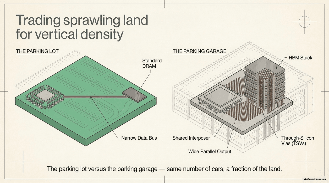
Ordinary DRAM, of the kind found in a laptop, plugs into the rest of the computer over a relatively narrow set of wires, and sits some distance away on the circuit board. That's efficient to manufacture and perfectly fine for everyday tasks. It is nowhere near fast enough to keep a modern AI GPU fed.
HBM: A Parking Garage Instead of a Parking Lot
The fix the industry landed on is called HBM — High-Bandwidth Memory — and the easiest way to picture what it does differently is a parking analogy. Ordinary memory is like a sprawling single-story parking lot: to add capacity, you build outward, and every car still has to funnel through the same narrow rows to reach the exit. HBM is a parking garage: instead of spreading out, it stacks upward, and — crucially — it also builds a separate elevator shaft for every single row of cars, so thousands of cars can leave simultaneously through thousands of parallel exits rather than queuing for one.
Physically, that means HBM takes several individual DRAM chips — often 8, 12, or more — and stacks them directly on top of one another into a single tower, connected top to bottom by thousands of microscopic vertical wires drilled straight through the silicon, called through-silicon vias (TSVs). Instead of data trickling out through a narrow set of side connections, it can flow out of thousands of vertical channels at once, all through the bottom of the stack. That whole tower is then placed directly onto the interposer next to the GPU die, using the same CoWoS-style packaging from Section 2.1 — which is precisely why packaging and memory turned out to be tangled up with each other. HBM isn't just faster memory; it's memory redesigned, from the ground up, to be assembled inches away from the chip it feeds, using an entirely different packaging technique than the DRAM in a laptop.
Drilling those through-silicon vias is itself a delicate operation, and it's worth understanding why HBM can't simply be made faster by stacking more dies. Each via has to be etched straight down through a die that has already been thinned to a fraction of the thickness of a sheet of paper, without cracking it, and then precisely aligned with the matching via on the die below and above it — thousands of times per stack, with essentially zero tolerance for misalignment. Stack too many dies, or push the vias too close together, and the odds of a single bad connection ruining the whole tower start to climb, the same yield problem chiplets ran into in Section 2.1. That's a large part of why HBM stack heights have grown gradually — 4 dies, then 8, then 12 and beyond — rather than jumping straight to whatever height would be theoretically fastest. Every additional layer is a manufacturing achievement in its own right, not just a bigger number on a spec sheet.
Why HBM Is Scarce
Only three companies in the world currently manufacture HBM at meaningful volume: Micron, Samsung, and SK Hynix. Micron is the only one of the three headquartered in the United States. That's an extraordinarily small number of suppliers for a component now considered essential to every AI server built. Building the capacity to make HBM isn't something a company can do quickly — it requires new fabrication lines, new packaging know-how, and years of qualification testing with GPU makers before a memory maker's stacks are trusted to ship in volume. Demand for HBM has been growing far faster than that capacity can be added: industry estimates put the HBM market at roughly $35 billion in 2025, with expectations it could reach roughly $100 billion by 2028. That kind of demand growth, running into a three-supplier ceiling, is part of why memory prices across the whole industry — not just HBM, but conventional DRAM and flash storage too — have surged sharply, with reported DRAM contract prices climbing in the mid-60% range and flash-memory (the electronic storage chips inside solid-state drives — more on those in section 2.3) prices climbing in the high-70% range within a single quarter in 2026. Memory has become, in the words used across the industry in 2026, the universal bottleneck of AI hardware — the one ingredient that constrains almost every server build, no matter which GPU maker or server assembler is involved.
When Each Kind of Memory Is Used
HBM is not a universal replacement for ordinary DRAM — it's dramatically more expensive to produce, given the stacking and packaging involved, so it's reserved specifically for sitting immediately beside the highest-performance compute chips: GPUs and other AI accelerators, where the memory-bound bottleneck described above is most severe. Conventional DRAM — cheaper, simpler, mounted the traditional way — still does the vast majority of the world's everyday computing: the CPU's own working memory, servers running ordinary business software, laptops, phones. The two aren't competing for the same job. HBM exists because one specific job — feeding a GPU fast enough — became impossible any other way.
Storage — The Filing Cabinet
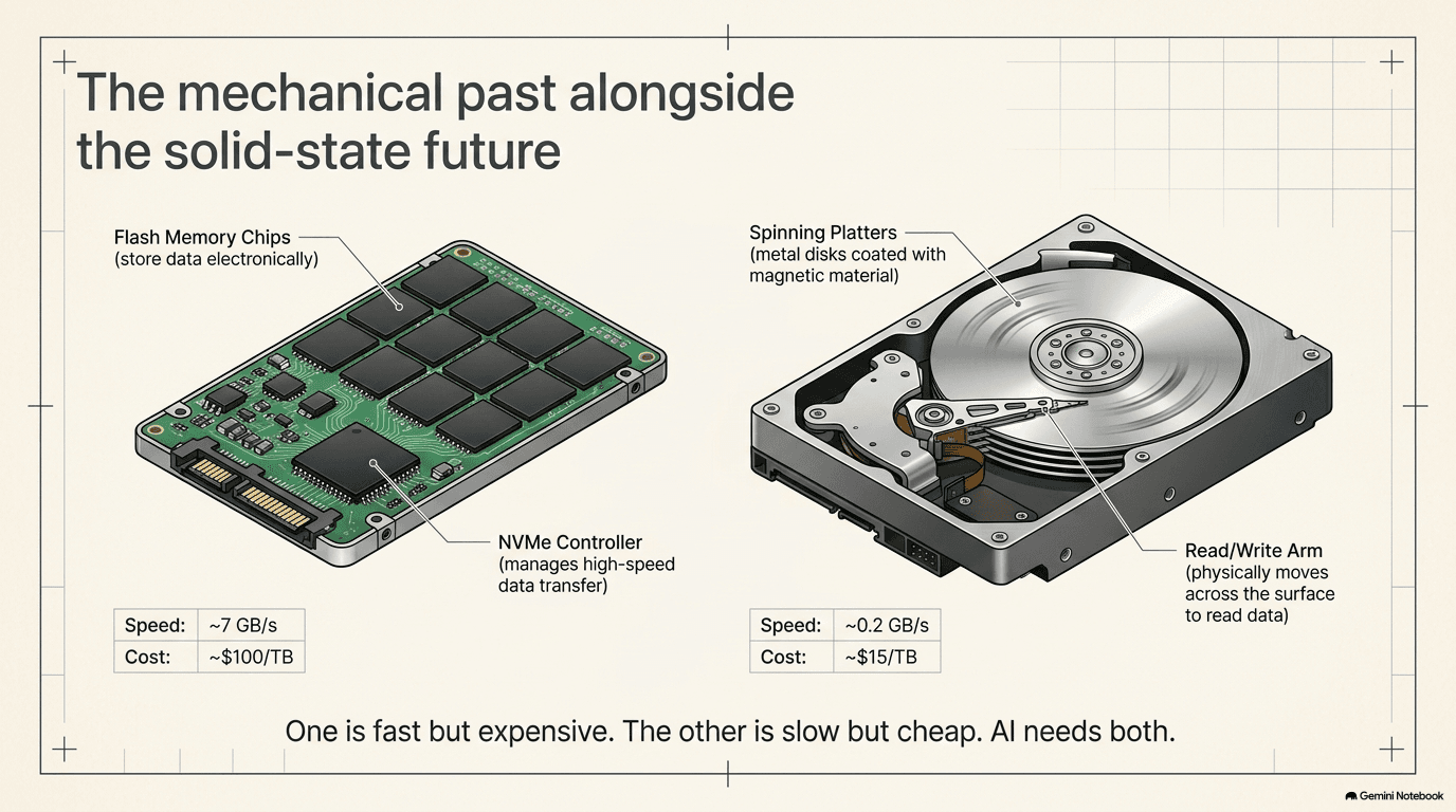
Memory and storage are often confused, but they solve opposite problems. Memory (2.2) is fast and temporary — the scratch paper that vanishes the instant the power turns off. Storage is slower but permanent — the filing cabinet where things are kept even with the lights out. A chip pulls a number out of storage, works on it in memory, and eventually writes a result back to storage to keep.
There are two basic kinds of storage hardware. A hard disk drive (HDD) stores data magnetically on a set of spinning metal platters, read by a tiny arm that physically moves across the surface — mechanically, it's not so different from an old record player. It's slow relative to memory, because a physical arm has to move and a physical disk has to spin to the right spot, but it's cheap per unit of storage, which makes it the choice for storing enormous volumes of data that don't need to be retrieved instantly. A solid-state drive (SSD) has no moving parts at all — it stores data electronically, in flash memory chips, the same broad technology family as a USB thumb drive but engineered for much higher speed and durability. SSDs are far faster than spinning disks but cost more per unit of storage, so they're used where speed matters more than raw capacity. A common connection standard for fast SSDs is called NVMe, which is simply the modern high-speed "road" data travels down between a flash chip and the rest of the server — a wider, faster version of the older roads storage used to travel over.
AI needs both kinds, for different reasons, and in enormous quantities. Training a large AI model starts with a training dataset that can run to many trillions of words, images, or other examples — far too much to fit in memory at once, so it lives in bulk storage and gets pulled in during training, piece by piece. That bulk role tends to fall to hard drives, because the sheer volume needed makes cost per unit the deciding factor; drive makers are pushing hard drive capacity past 40 terabytes per drive using a technique called HAMR (heat-assisted magnetic recording), which briefly heats a tiny spot on the disk with a laser immediately before writing to it, allowing data to be packed more tightly than a drive could reliably read and write at room temperature alone. Faster SSD storage, meanwhile, tends to sit closer to the actual computing — holding checkpoints of a model mid-training, or serving up data that needs to be fetched quickly and repeatedly.
There's also a newer, self-reinforcing pattern often called the data loop. Historically, most of the data used to train AI models was created by humans over decades — books, websites, photographs. Increasingly, AI systems themselves generate enormous volumes of new data simply by being used: every response an AI model gives, every image it generates, every action an AI "agent" takes while completing a task, is itself new data. Some of that gets captured, reviewed, and cycled back into training the next generation of models. In other words, running AI inference — actually using a trained model to answer questions or complete tasks — doesn't just consume storage; it also creates new storage demand, which is part of why storage needs have kept expanding even as models themselves mature.
None of this storage sits inside a single server, either. Training a large AI model spreads work across thousands of servers at once (Chapter 3 explains how they're networked together), and all of those servers typically need to read from — and write to — the same enormous pool of data at the same time, not thousands of separate private copies. That job falls to a parallel file system: shared storage, built from many drives working together, engineered specifically so that thousands of servers can request different pieces of the same dataset simultaneously without the whole system grinding to a crawl the way a single hard drive would if a thousand people tried to read from it at once. Storage, in an AI data center, behaves less like a filing cabinet sitting in one office and more like a library built to be read by an entire city simultaneously.
What Is a Server?
Strip away the mystique, and a server is simply a computer built to do one thing without a screen, a keyboard, or a person sitting in front of it, running continuously, day and night, for years. Where a laptop is designed around comfort — a nice keyboard, a bright screen, quiet fans, a battery that sips power — a server is designed entirely around throughput and reliability: cram in as much computing power as physically possible, keep it running nonstop, and make it serviceable by a technician in a data center rather than pleasant to hold on your lap.
Physically, a server is a metal box, usually a few inches tall and wide enough to slide into a standard-width steel frame called a rack — the same racks visible in almost any data center photo, holding row after row of identical boxes stacked one above another. Chapter 4 covers the server and the rack it lives in more fully; this section is about what's inside the box itself.
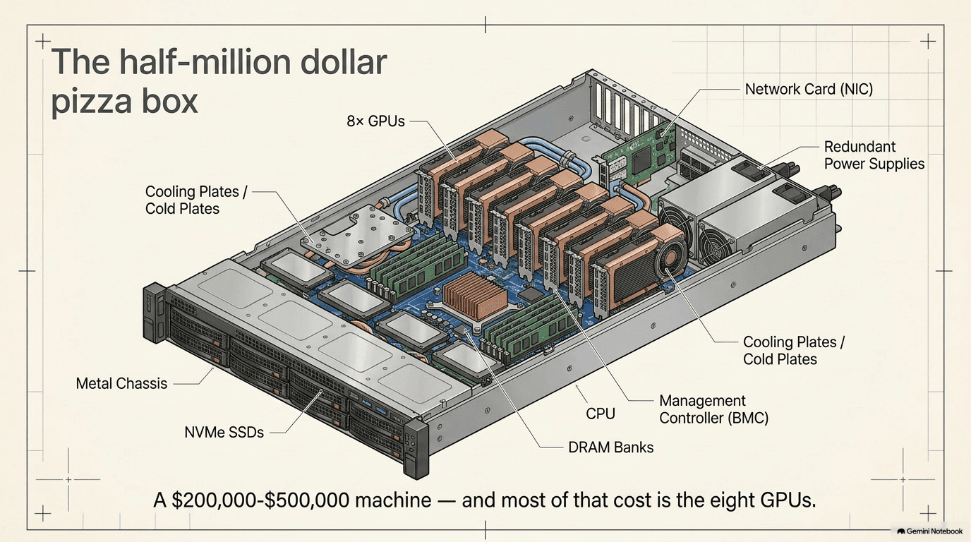
Open one up, and an AI server contains, at minimum:
- The GPUs — typically eight or more of them in a single AI server, each one the "thousand hammers" chip from Chapter 1, doing the actual AI computation.
- A CPU — the "Swiss Army knife" chip from Chapter 1, which doesn't do the heavy AI math itself but manages the overall system: booting the machine, coordinating tasks, and handing work off to the GPUs.
- Memory — both the HBM riding right on each GPU package (2.2) and separate, larger pools of ordinary DRAM serving the CPU.
- Storage — SSDs, sometimes HDDs, for holding data and model checkpoints (2.3).
- A network card — the component that lets this server talk to every other server in the data center at extremely high speed, because AI training is almost never done on a single machine; it's spread across thousands of servers working together. Chapter 3 covers networking.
- Power supplies — components that take in the electricity delivered by the data center and convert it into the specific voltages every other part inside the server needs. Section 2.6 covers what happens after that conversion.
- Fans, or in newer designs, liquid cooling plumbing — because eight or more GPUs, each drawing hundreds of watts, generate a tremendous amount of heat in a very small space. Chapter 6 covers cooling in full.
- A management controller — a small, separate, low-power chip that watches over the rest of the server independently of everything else — monitoring temperatures, fan speeds, and power draw, and giving a remote technician a way to restart or diagnose the machine even if the main system has crashed entirely. It's the server's own black box: a minder that stays awake and reachable no matter what state the rest of the machine is in.
A fully loaded AI server, of the kind used to train or run the largest AI models, typically costs somewhere in the range of $200,000 to $500,000. The overwhelming majority of that cost is the GPUs themselves — eight or more of the world's most advanced, most expensive chips, sitting inside one box. Everything else described in this chapter — the packaging, the memory, the board, the power delivery — exists to let those GPUs actually do useful work, rather than sit next to each other unable to communicate fast enough to matter.
The Motherboard — The Road Map
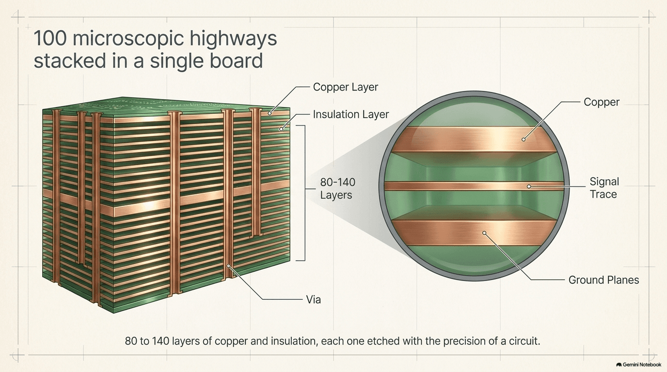
Every component inside a server has to physically connect to every other component, and the thing they all plug into is the motherboard: a flat board, built up out of many thin layers of copper wiring sandwiched between layers of fiberglass-like insulation, that carries both electrical power and digital signals to every chip mounted on it. If a chip is a city, the motherboard is the entire road network connecting every building in that city to every other one.
An ordinary laptop or desktop motherboard might have somewhere around 8 to 12 layers of copper wiring buried inside it. An AI server board is a different animal entirely. Because it has to route power and extremely high-speed data signals to eight or more GPUs, plus a CPU, plus multiple memory pools, plus network connections, all without any of those thousands of individual "roads" crossing or interfering with each other, the layer count on modern AI boards has been climbing steadily — from roughly 80 layers, to 100, to boards now reaching around 140 layers. Each additional layer adds cost and manufacturing complexity, because every layer has to be etched, aligned, and bonded with extreme precision — but there's often no other way to fit all the necessary connections into the available space without one signal's electrical "road" crossing another's and causing interference, the electronic equivalent of two radio stations bleeding into each other on the same frequency.
That interference problem is worth understanding a little more concretely, because it's the reason board design has become its own engineering specialty. At the speeds these signals move — billions of times per second — a copper trace on a board doesn't just carry electricity the way a garden hose carries water; it starts to behave like an antenna, radiating a faint signal of its own that can bleed into any neighboring trace running close by and roughly parallel to it. Route two high-speed lines too near each other, or let a trace's width vary unevenly along its length, and one signal can corrupt another before it even reaches its destination — silently turning a correct 1 into a corrupted 0 somewhere along the way. Engineers manage this with a discipline called signal integrity: carefully controlling the width, spacing, and surrounding material of every trace so its electrical behavior stays predictable and clean along its entire length, and separating especially sensitive lines onto their own dedicated layers, insulated above and below by solid sheets of copper that act like a shield. It's a large part of why simply adding more layers isn't a free way to solve every routing problem — every new layer of high-speed signals needs its own layer of shielding around it, which is one reason layer counts keep climbing rather than leveling off.
Scattered across the surface of that board, by the thousands, sit tiny components called passives — resistors, and especially capacitors. A capacitor, as described in 2.2, briefly stores a small amount of electrical charge; on a motherboard, banks of them sit right next to each power-hungry chip and act as tiny local reservoirs, smoothing out the electricity flowing into the chip so it doesn't spike or dip as the chip's demand for power changes instant to instant — similar to how a small water tank on a rooftop keeps water pressure steady even as different taps in a house turn on and off unpredictably. A single modern GPU board can carry thousands of these multi-layer ceramic capacitors (MLCCs), each one individually tiny but collectively essential to keeping power delivery stable.
Power on the Board — Squeezing Down to One Volt
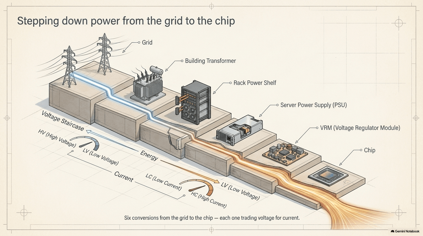
Electricity arrives at a data center at a relatively high voltage, because high voltage is the efficient way to move large amounts of power over any real distance — the same reason long-distance power lines run at extremely high voltage, then get stepped down closer and closer to the building before reaching a wall socket. That same principle repeats at a much smaller scale on the way into a single chip.
By the time power finally reaches the GPU itself, it needs to arrive at roughly one volt — a tiny, precise trickle, compared to the voltage running through the rack around it. Getting from "rack-level" voltage down to "one volt at the chip" is the job of a component called a voltage regulator module, or VRM: a small cluster of components, sitting on the board immediately next to the GPU, that continuously steps voltage down and holds it rock-steady, adjusting many times per second as the chip's power demand shifts with what it's computing.
The Current Problem
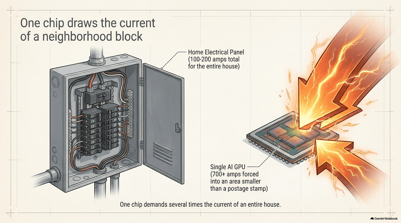
Here's where the numbers get genuinely strange. Power, in simple terms, is voltage multiplied by current. If voltage is like water pressure (how hard the electricity pushes), current is the flow rate (how much electricity is actually moving through the wire at any given moment, measured in units called amps). A modern AI GPU can draw 700 watts or more, and next-generation chips are heading toward 1,000 to 1,200 watts each. If that power has to arrive at only about one volt, then by simple arithmetic the current has to be enormous — over 700 amps, in some cases, flowing into a single chip roughly the size of a fingernail. For comparison, a typical American home's entire electrical panel is rated for somewhere around 100 to 200 amps total. One AI chip can be asked to accept several times the current capacity of an entire house, delivered into an area smaller than a postage stamp. Doing that without melting anything, and without the voltage sagging the instant the chip's demand spikes, is one of the genuinely hard engineering problems in a modern AI server — every VRM has to be extraordinarily fast and precise, and every connection carrying that current has to be sized to handle it without overheating.
Why the Industry Is Moving to 800-Volt Racks
One way to ease this problem is to avoid stepping voltage down so far, so late. For years, data center racks distributed power internally at a relatively low 48 volts. The industry — pushed heavily by NVIDIA — is now shifting toward distributing power inside the rack at a much higher 800 volts DC (direct current, meaning the electricity flows steadily in one direction, rather than the back-and-forth alternating current, AC, that comes out of a wall socket). Distributing power at a higher voltage inside the rack means a smaller final step-down is needed at each individual server board, which reduces how much current has to be carried through the highest-loss part of the journey, and cuts down on the sheer thickness of copper cabling needed to move that power around a data center full of racks. It's the same "high voltage travels efficiently" principle from the start of this section, simply applied one level closer to the chip than it used to be.
This is not a small change to make. Retooling a rack's entire power architecture around a new, much higher voltage standard means new power supplies, new cabling, and new safety systems throughout the data center — which is why the shift, though underway, has meaningfully changed the cost of building out a rack. A traditional 120-kilowatt rack has historically carried something on the order of $9,500 worth of power-related content. An 800-volt rack of the new kind carries something closer to $115,000 — roughly a twelvefold jump — reflecting how much more sophisticated the entire power delivery chain has to become to handle both the higher voltage and the sheer amount of power a rack full of next-generation AI servers now demands.
New Materials for Switching Power
Stepping voltage down efficiently, at these speeds and currents, has also pushed the industry toward newer semiconductor materials for the switching components inside VRMs and power supplies. Traditional power electronics are built from silicon — the same base material as the chips in Chapter 1 — but two newer materials, gallium nitride (GaN) and silicon carbide (SiC), can switch on and off faster and waste less energy as heat while doing it, particularly at higher voltages like the emerging 800-volt standard. The underlying reason is that both materials can withstand a much stronger electric field than silicon before breaking down, which lets a component built from them be made physically smaller for the same job, switch on and off more times per second, and let less energy leak away as waste heat during each switch. Losing less energy to heat during the voltage-conversion step matters twice over: it means more of the electricity a data center pays for actually reaches the chip to do useful computing, and it means less extra heat that the cooling system (Chapter 6) then has to remove — and every watt not wasted in the power stage is a watt the liquid cooling loop doesn't have to carry away later.
Who Assembles It All
A finished GPU, wrapped in its CoWoS package with HBM riding alongside it, is still just one part among many. Someone has to design the motherboard it plugs into, mount every component onto that board, wire in the power delivery system described above, install the cooling, and build the whole thing into a chassis that can slide into a rack. That final assembly step is split, broadly, between two kinds of companies.
An OEM (original equipment manufacturer) designs a server, puts its own brand name on it, and sells it — the company a customer actually buys the finished machine from. Dell is the largest server maker in the world by revenue, selling broadly across both traditional enterprise computing and AI systems. Super Micro has built its business almost entirely around AI: the large majority of its revenue now comes specifically from AI GPU server platforms, making it one of the purest bets in the public market on AI server demand itself, rather than one line of business among many.
Sitting behind many of the brand names customers actually see, contract manufacturers physically build servers designed by someone else — sometimes an OEM, sometimes a large customer that designs its own hardware in-house and simply needs someone to build it at scale. Celestica manufactures the custom TPU (Tensor Processing Unit — Google's own purpose-built AI chip, playing the same role a GPU does but designed specifically for Google's data centers) systems Google designs for its own AI computing. Flex builds the new generation of 800-volt power racks for NVIDIA's newest systems. Both companies are, in effect, invisible to the end customer — the finished product may carry another company's name — but without their factories, the design on paper never becomes a physical machine.
Laid end to end, the path from raw silicon to a working AI server now runs through an unusually long chain of specialists, each one a potential chokepoint of its own: a chip designer creates the blueprint; a foundry etches it onto a wafer (Chapter 1); a packaging house gives the finished die a body and welds it next to its memory (2.1); a small handful of memory makers supply that memory in the first place (2.2); a board maker builds the motherboard it all plugs into (2.5); a power-electronics supply chain gets electricity down to the one volt the chip actually needs (2.6); and finally an OEM or contract manufacturer assembles everything into the finished box that ships to a data center. As of 2026, the single tightest link in that entire chain is memory — HBM in particular — with demand from AI systems running well ahead of the three companies in the world capable of supplying it. A server can have every other part ready and waiting, and still sit unfinished for want of memory stacks.
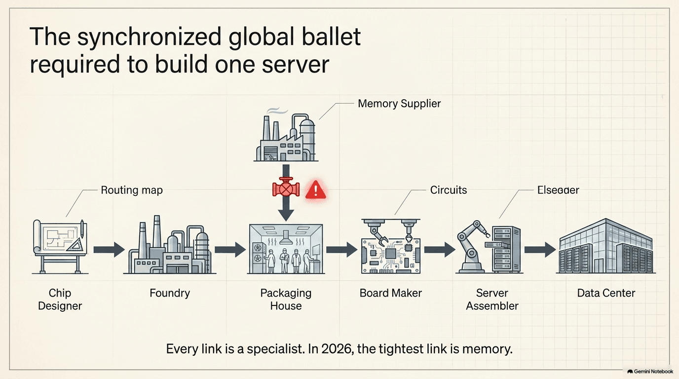
Chapter 3 picks up from here and follows the network cable out of the back of the server — how thousands of these machines, each one built exactly as described in this chapter, are wired together to work as a single enormous computer.
Companies in this part of the buildout: Servers & Compute, Silicon Design, Chip Making