Chapter 1
The Chip
A chip is a tiny piece of silicon with billions of microscopic switches etched into it — and building one requires the most precise manufacturing process humans have ever invented.
What Is a Chip?
Pick up your phone. Somewhere inside it, no bigger than your thumbnail, sits a chip. It's a thin sliver of silicon — the same element found in ordinary sand — with billions of tiny electrical switches carved into its surface. Each switch is called a transistor. A transistor does one simple thing: it turns on or it turns off. On means "1." Off means "0." Every photograph you've taken, every message you've sent, every video you've watched — all of it is just transistors switching on and off, billions of times per second.
The first transistor, built in 1947, was the size of your palm. Today, a single chip holds more transistors than there are stars in the Milky Way. An NVIDIA H100 — one of the chips powering most of today's AI systems — packs 80 billion transistors onto a piece of silicon smaller than a postage stamp. It's built on a manufacturing process from TSMC in what the industry calls the "5-nanometer class." A quick warning about those names: labels like "5-nanometer" or "3-nanometer" are industry shorthand, not measurements — they stopped describing the actual size of anything on the chip years ago. What's true is that the smallest features on a modern chip are only a few nanometers across. A nanometer is one-billionth of a meter — so small that tens of thousands of these features would fit across the width of a single human hair.
Why does smaller matter? Three reasons. First, smaller transistors switch faster — the electrons have less distance to travel. Second, you can fit more of them onto the same piece of silicon, which means more computing power per chip. Third, smaller transistors use less energy per switch. When you're switching billions of them billions of times per second, that energy savings is the difference between a chip that runs cool and one that melts.
CPUs and GPUs: Two Different Machines
Not all chips think the same way. The two most important kinds are CPUs and GPUs.
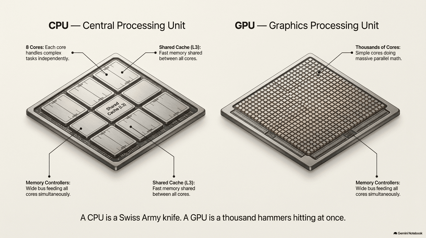
A CPU — central processing unit — is what runs your laptop. It has a small number of very powerful cores (typically 8 to 24), and each core can handle a complex task on its own. A CPU is a Swiss Army knife: it can do almost anything, one thing at a time, and do it well. When you open a spreadsheet, your CPU is doing the work.
A GPU — graphics processing unit — works differently. Instead of a few powerful cores, it has thousands of small, simple ones. Each individual core is weaker than a CPU core, but together, working in parallel, they can do an enormous amount of simple math all at once. A GPU is not a Swiss Army knife. It's a thousand hammers hitting at the same time.
This parallel structure is why GPUs turned out to be the engine of artificial intelligence. Training an AI model — a process called "machine learning" — involves multiplying enormous tables of numbers together, billions of times, to slowly adjust the model's behavior. Each individual multiplication is simple. But there are so many of them that a CPU, doing them one at a time, would take months. A GPU, doing thousands at once, can finish in days.
NVIDIA (NVDA) designs the GPU that dominates AI computing. Their chips — the A100, then the H100, and now the Blackwell generation — are the standard hardware for training large AI models. AMD (AMD) is the primary competitor, with its Instinct MI series. Intel (INTC), which dominated computing for decades with its CPUs, is working to catch up in AI chips. And increasingly, the largest cloud companies — Amazon, Google, Microsoft — are designing their own custom AI chips, manufactured for them by dedicated chip factories called foundries (we'll get to foundries shortly). Broadcom (AVGO) and Marvell (MRVL) are two of the main companies that help hyperscalers design these custom chips.
Designing a Chip
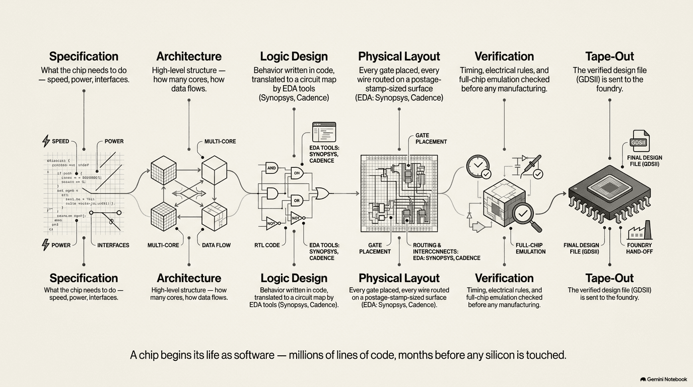
A chip starts its life not as a physical object, but as a file. Specifically, a design file — an extraordinarily detailed set of instructions that describes where every transistor, wire, and connection on the chip should go. Creating that file is the work of chip design, and it's done entirely in software.
The Software: EDA Tools
The software used to design chips is called EDA — electronic design automation. Think of it as AutoCAD for circuits, except the "building" you're designing has billions of components, all of which must work together at speeds measured in billionths of a second.
Two companies dominate EDA: Synopsys (SNPS) and Cadence (CDNS). Between them, they provide the software that virtually every advanced chip in the world is designed with. Synopsys is the larger of the two, with roughly $9.7 billion in annual revenue. It recently acquired Ansys for $35 billion, adding the ability to simulate heat, airflow, and electromagnetic interference — problems that become critical when you're packing billions of transistors into a space the size of a postage stamp. Cadence, at roughly $6.2 billion in revenue and growing faster organically (its core EDA business grew 18% year-over-year versus Synopsys's 8%), provides a competing suite of tools that covers the same ground — design, verification, layout, and simulation. Cadence's Palladium Z3 emulation system — a specialized piece of hardware that runs a simulation of the chip's behavior in real time, far faster than software alone — can verify chip designs with up to a trillion transistors, far beyond what any current chip contains, which gives a sense of where complexity is headed. No advanced chip gets built without passing through one of these two companies' tools.
Smaller competitors exist — Siemens has an EDA division, and Chinese startups are building domestic alternatives — but at the leading edge, the Synopsys-Cadence duopoly is effectively unchallenged. No single customer exceeds 10% of Cadence's revenue. For Synopsys, one unnamed customer accounts for 12.6%.
How a Chip Gets Designed: From Idea to Layout
The design process follows a sequence of steps, each handled by different EDA tools:
Step 1 — Specification. The chip company decides what the chip needs to do. How many transistors? How fast? How much power can it consume? What interfaces does it need — memory controllers, input/output ports, communication links?
Step 2 — Architecture. Engineers define the chip's high-level structure: how many cores, how they're connected, where the memory interfaces go, how data flows through the system.
Step 3 — Logic design. Engineers write the chip's behavior in a hardware description language (a specialized programming language that describes circuits, not software). This description says what the chip does, not how it's physically built. EDA synthesis tools (like Synopsys's Fusion Compiler or Cadence's Genus) then translate this description into a "netlist" — a map of specific logic gates (the building blocks made from transistors) and how they connect.
Step 4 — Physical layout. Place-and-route tools (like Cadence's Innovus) take the netlist and assign every gate a physical location on the chip, then draw the wires connecting them. This is staggeringly complex — imagine arranging billions of components on a surface smaller than a postage stamp, then routing millions of wires between them, all while ensuring the electrical signals arrive at the right time and nothing overheats. For the most advanced AI chips, this step alone can take months of compute time.
Step 5 — Verification and signoff. Before any physical manufacturing begins, the design must be verified. Timing analysis tools (Synopsys PrimeTime, Cadence Tempus) confirm that every signal in the chip arrives when it should. Physical verification tools check that the layout follows the manufacturing rules of the target foundry — the minimum wire widths, spacing, and layer alignments. For billion-transistor AI chips, teams also use emulation hardware — physical machines that simulate the chip's behavior in real time — to test the design before committing to manufacturing. A single error caught at this stage costs hours of engineering time. The same error caught after manufacturing costs millions.
Step 6 — Tape-out. The verified design is exported as a file (in a format called GDSII or OASIS) and sent to the foundry — the factory that will manufacture the physical chip. This moment is called "tape-out," a term from the era when designs were literally sent on magnetic tape.
Pre-Built Pieces: IP Blocks
Not everything in a chip is designed from scratch. Chip designers license pre-designed components called IP blocks (intellectual property blocks). Think of these as off-the-shelf engines that you drop into a custom car frame. A chip might license a USB interface from one company, a memory controller from another, and a processor core from a third — then connect them all with custom logic.
The most important IP company in the world is Arm (ARM). Arm doesn't manufacture chips. Instead, it designs processor core architectures and licenses them to chip makers, who pay an upfront fee plus a royalty on every chip shipped — typically a few cents per chip, but across billions of devices, it adds up. In its fiscal year 2026, Arm reported $4.9 billion in revenue: $2.6 billion from royalties and $2.3 billion from licensing fees. Nearly every smartphone processor in the world uses Arm's architecture. And increasingly, AI chips and data center processors are built on Arm designs too — Arm's data center royalties more than doubled year-over-year. The company has publicly stated a long-term target of $25 billion in revenue by fiscal year 2031.
In March 2026, Arm took an unusual step: it entered the chip business directly, announcing its own 136-core AGI CPU. This puts it in partial competition with the very companies it licenses to — a significant shift for a company that has historically been a neutral supplier to the entire industry.
Arm licenses the processor's brain. Other IP companies specialize in the surrounding functions. CEVA (CEVA), for instance, licenses the designs for wireless connectivity (Bluetooth, Wi-Fi, cellular), sensing, and small AI-processing blocks that chipmakers embed into their own designs — the kind of intelligence that goes into the billions of connected devices at the edge of the network. Like Arm, CEVA doesn't manufacture chips; it earns an upfront license fee plus a royalty on every chip shipped with its IP inside.
Making the Silicon — Sand to Wafer
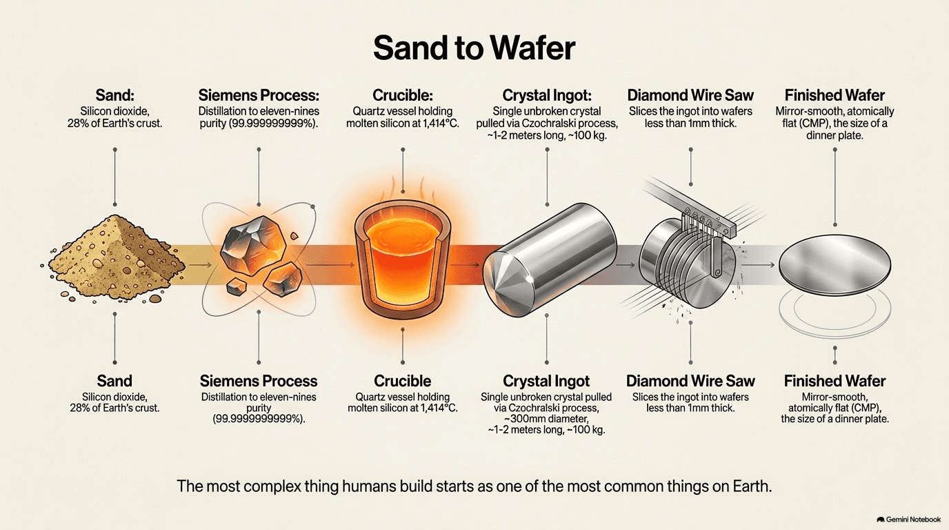
Every chip in the world starts as sand. Specifically, it starts as silicon dioxide — the same compound that makes up most beach sand and about 28% of the Earth's crust. Silicon is the second most abundant element on the planet after oxygen. It's everywhere. The challenge isn't finding it. The challenge is making it pure enough.
Purification: From Sand to Electronic-Grade Silicon
Ordinary sand is about 95% silicon dioxide, mixed with iron, aluminum, calcium, and dozens of other elements. To make chips, you need silicon that is 99.999999999% pure — that's "eleven nines," meaning for every hundred billion atoms of silicon, fewer than one can be anything else. A single stray atom of the wrong element in the wrong place can ruin a transistor.
The purification happens in stages. First, the sand is heated with carbon in an electric arc furnace at roughly 2,000°C. The carbon pulls the oxygen away from the silicon, leaving behind metallurgical-grade silicon — about 98% pure. Good enough for making steel. Not nearly good enough for chips.
Next comes the Siemens process (named after the company that developed it, not the modern conglomerate). The impure silicon is converted into a gas — trichlorosilane — by reacting it with hydrogen chloride. This gas is then distilled, much like whiskey, to separate the silicon from the remaining impurities. Different impurities boil at different temperatures, so repeated distillation stages remove them one by one. Finally, the purified gas is deposited onto heated silicon rods in a sealed reactor, where it decomposes back into solid, ultra-pure silicon. The result: polycrystalline silicon, or "polysilicon" — irregular chunks of silicon pure enough for semiconductor manufacturing.
Crystal Growth: The Czochralski Process
Polysilicon is pure, but its atoms are jumbled — arranged in random grains, like the crystal structure of a rock. Chips need silicon where every atom is in a perfect, unbroken crystal lattice — a single crystal, with no grain boundaries. To get this, you melt the polysilicon and grow a crystal.
The standard method, used since the 1950s, is the Czochralski process (named after the Polish chemist who invented it — the name is pronounced roughly "cho-KRAL-ski"). Here's how it works:
Ultra-pure polysilicon chunks are loaded into a quartz crucible and heated to about 1,414°C — silicon's melting point. A small seed crystal, about the size of a pencil, is dipped into the molten silicon and then slowly pulled upward while rotating. As the seed rises, silicon atoms from the melt attach to it, continuing the seed's crystal structure. Over the course of several hours to days, a cylindrical ingot grows — a single, unbroken crystal of silicon, typically about 300 millimeters (12 inches) across and one to two meters long. It weighs roughly 100 kilograms.
The 300mm diameter is important: it's the standard wafer size used in all modern chip factories. A bigger wafer means more chips per wafer, which lowers the cost per chip. The industry settled on 300mm in the early 2000s; moving to a larger size (450mm has been discussed for decades) would require redesigning every piece of equipment in every factory, at a cost of hundreds of billions of dollars. No one has done it.
Slicing and Polishing
The crystal ingot is sliced into individual wafers using a wire saw — a fine wire coated with diamond particles. Each wafer is less than a millimeter thick. After slicing, the wafers are polished to an atomic-level flatness using a process called CMP — chemical-mechanical planarization (or polishing). The wafer's surface must be so flat that if you scaled it up to the size of a football field, the largest bump would be less than a millimeter high.
The result is a blank wafer: a perfectly flat, perfectly pure, mirror-smooth disk of silicon, the size of a dinner plate, ready to have circuits printed onto it.
Who Makes Wafers
This step of the process is dominated by companies outside our universe — the major wafer suppliers are Shin-Etsu Chemical and SUMCO (both Japanese), along with Germany's Siltronic and smaller players in South Korea and Taiwan. Within our coverage, Ferroglobe (GSM) produces silicon metal — the refined elemental silicon that serves as the feedstock for polysilicon (and for silicones) — rather than finished wafers. The more exotic materials used in power electronics, like silicon carbide, come up in Chapter 10 (The Materials).
Printing the Pattern — Photolithography
A blank wafer is like a blank page. The patterns of billions of transistors, wires, and connections that make up a working chip have to be printed onto its surface — one layer at a time, with a precision that makes every other manufacturing process on Earth look crude.
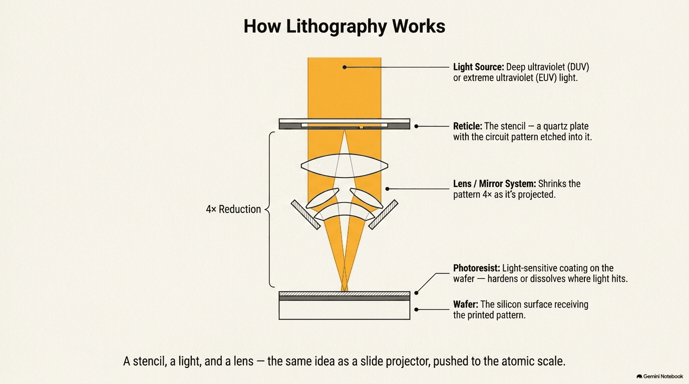
The technology that does this is called photolithography. At its core, it works like an old-fashioned photograph. You coat the wafer in a light-sensitive chemical (called a photoresist), shine a carefully shaped beam of light through a stencil of the pattern you want, and the light changes the chemical wherever it hits. Then you wash the wafer with a solvent: the unexposed resist stays, the exposed resist dissolves (or vice versa, depending on the type), and the pattern is left behind on the wafer surface. That pattern is then used as a mask for the next step — etching trenches, depositing metal, or building up another layer of the chip.
This basic concept hasn't changed since the 1960s. What has changed, dramatically, is the light.
The Wavelength Problem
Photolithography can only print features as small as the wavelength of light used to print them. Just as you can't write your name with a paintbrush the size of a broom, you can't print transistors smaller than your light beam using basic optics. (In practice, engineers have pushed well past this limit using clever tricks, but the fundamental physics creates a floor.)
For decades, the industry used deep ultraviolet (DUV) light with a wavelength of 193 nanometers — invisible to the human eye, far shorter than visible light, and produced by excimer lasers. DUV lithography, combined with tricks like immersion (putting a layer of water between the lens and the wafer to bend the light more tightly) and multiple patterning (printing the same layer multiple times with slightly shifted patterns), took the industry from 90-nanometer features down to about 7 nanometers. That's roughly 1/10,000th the width of a human hair.
But DUV hit a wall. To print features smaller than 7 nanometers reliably, you'd need so many patterning passes that the cost and time became prohibitive. The industry needed shorter light.
EUV: Extreme Ultraviolet Lithography
The answer was EUV — extreme ultraviolet light, with a wavelength of 13.5 nanometers. That's about 14 times shorter than DUV light, which means it can print features 14 times finer in a single pass. But getting light this short to work in a manufacturing tool was one of the hardest engineering problems of the 21st century.
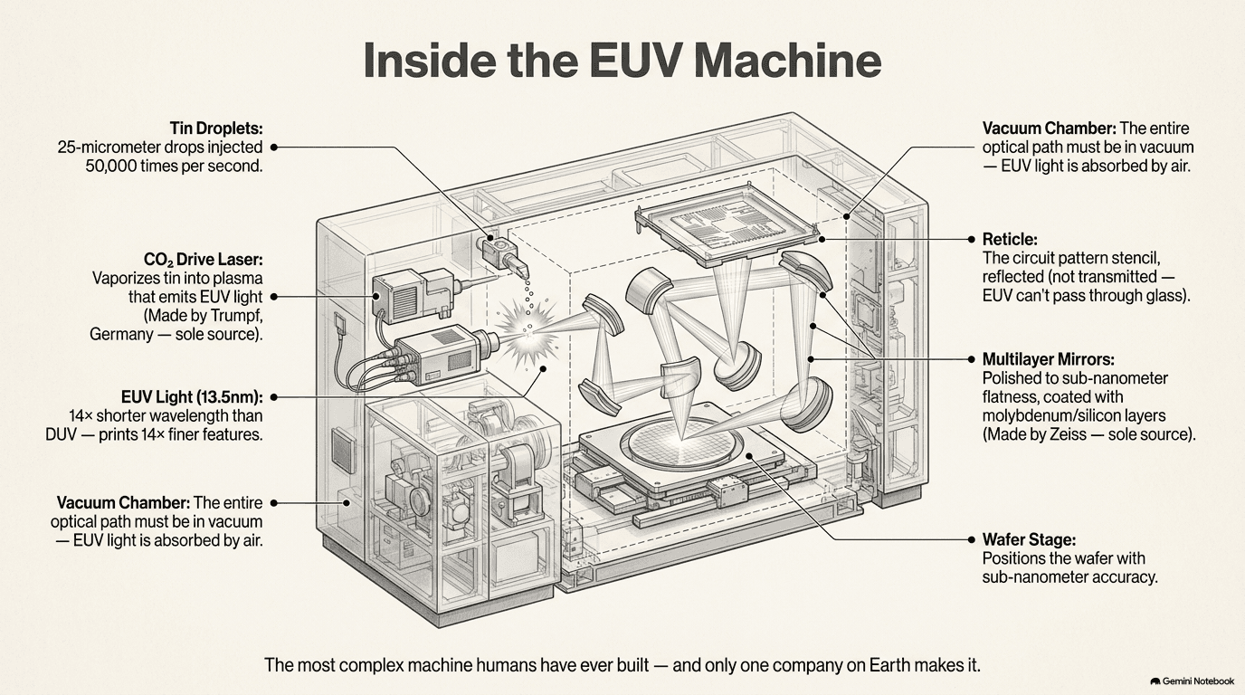
Here's the first problem: EUV light is absorbed by everything. It's absorbed by air. It's absorbed by glass. You can't use a traditional lens system — the light would never make it through. Instead, the entire optical path must use mirrors, not lenses, and the whole system must operate in a near-perfect vacuum.
Here's how an EUV lithography machine works:
The light source. A stream of microscopic tin droplets — each about 25 micrometers across, smaller than a grain of pollen — is injected into a vacuum chamber. A powerful carbon dioxide laser fires at each droplet twice. The first pulse flattens the droplet into a thin disk. The second pulse, arriving microseconds later, vaporizes the tin disk into a plasma — a cloud of superheated, ionized gas — that emits extreme ultraviolet light. This happens 50,000 times per second. The laser system was developed by Trumpf, a German company, and is one of the critical sole-source components in the machine.
The mirrors. The EUV light is collected and focused by a series of multilayer mirrors — surfaces polished to a flatness of less than half a nanometer, coated with alternating layers of molybdenum and silicon, each layer precisely a few nanometers thick. These mirrors are made by Carl Zeiss SMT, a division of the German optics company Zeiss. Zeiss is the only company in the world that can manufacture mirrors to this specification. No other supplier has ever attempted it at production scale. Every EUV machine ASML builds depends on Zeiss optics, and Zeiss makes these optics for no other customer. The relationship runs both ways: ASML is Zeiss's only customer for EUV optics, and Zeiss is ASML's only supplier. This is the primary production bottleneck for EUV: the number of machines ASML can build each year is limited by the number of optical columns Zeiss can produce.
The reticle. The shaped light passes through (actually reflects off — because EUV can't pass through glass) a reticle — the stencil that carries the circuit pattern for one layer of the chip. The reticle itself is a masterpiece of precision: a flat quartz plate with an ultra-thin patterned absorber layer, made by companies like Photronics (PLAB) and Toppan.
The projection. The reflected pattern is then projected onto the wafer surface, which is coated in EUV-specific photoresist — a chemical that hardens (or dissolves) when struck by 13.5-nanometer light. The pattern is typically reduced 4× as it's projected, so the features on the reticle are four times larger than what's printed on the wafer.
The wafer stage. The wafer sits on a precision stage that positions it with accuracy measured in fractions of a nanometer. The machine prints one rectangular area of the wafer (called a "field"), then the stage steps to the next position, and it prints again. This step-and-scan process repeats hundreds of times to cover the entire wafer. Each exposure takes a fraction of a second.
The result: a precisely printed pattern of features as small as a few nanometers, repeated across the wafer surface, ready for the next processing step.
One Company, One Machine
ASML Holding (ASML), based in Veldhoven, the Netherlands, is the only company in the world that manufactures EUV lithography machines. This is not because competitors tried and failed — it's because the machine required over 20 years and billions of dollars of research and development, co-funded by Intel, Samsung, and TSMC (who took equity stakes in the project), and assembled from components that themselves have no second source. The carbon dioxide drive laser comes exclusively from Trumpf. The optical column comes exclusively from Zeiss. The light source system is built by ASML's own subsidiary, Cymer (acquired in 2013). No other company has ever brought an EUV lithography system to production.
ASML's scale reflects this position. In the second quarter of 2026, ASML reported revenue of €9.3 billion — in a single quarter. For the full year, ASML has raised its guidance twice, now expecting €43-45 billion in total revenue at a gross margin of 54-56%. The company plans to ship approximately 65 EUV systems in 2026, and is increasing production to roughly 85 units in 2027 and potentially 110 in 2028 — all within its existing factory footprint, by optimizing production layouts and reducing cycle times. A new manufacturing campus is breaking ground in Veldhoven, but that capacity targets demand beyond 2028.
Each EUV system costs upwards of $150 million. The machines weigh about 180 metric tons and require multiple Boeing 747 cargo flights to deliver. A single machine contains over 100,000 parts from thousands of suppliers across dozens of countries. Installation at a customer's fab takes months.
ASML also makes DUV lithography systems — the workhorse tools used for less advanced chip layers and by fabs that don't need cutting-edge resolution. In DUV, ASML faces competition from Canon and Nikon, both Japanese. But in EUV, it stands alone.
High-NA EUV: The Next Generation
Even EUV has limits. As chips push below 3 nanometers, even 13.5-nanometer light needs help printing the finest features. The answer is High-NA EUV — "NA" stands for numerical aperture, a measure of how much light the optics can gather and focus. A higher numerical aperture means finer resolution.
ASML's first High-NA system, the TWINSCAN EXE:5200B, shipped in April 2025. In July 2026, Intel announced that it had entered high-volume manufacturing using High-NA EUV on its Intel 18A process node — the first production use of the technology anywhere in the world. ASML expects to recognize revenue on 4-5 High-NA systems in 2026.
High-NA requires an entirely new optical column from Zeiss — the two types of optics cannot substitute for each other. This means the Zeiss bottleneck applies separately to each generation: expanding Low-NA production doesn't help High-NA supply, and vice versa.
The Photoresist: Light-Sensitive Chemistry
The photoresist — the light-sensitive chemical coating applied to the wafer before lithography — is itself a precision product. It must respond to the specific wavelength of light being used, change its chemical properties uniformly across the entire wafer surface, and wash away cleanly to leave sharp pattern edges. For EUV lithography, the resist chemistry is different from DUV — the shorter wavelength interacts with matter differently, and new resist formulations have been developed specifically for 13.5nm light.
The major photoresist suppliers are Japanese: JSR, Tokyo Ohka Kogyo (TOK), and Shin-Etsu Chemical. Entegris (ENTG) recently signed an EUV cross-licensing agreement with JSR/Inpria (May 2026), signaling that resist chemistry remains an active area of development and competition.
Why Lithography Is the Hinge
Every other step in chipmaking — design, deposition, etching, inspection, packaging — matters enormously. But lithography is the step that defines what's possible. The resolution of the lithography system sets the minimum feature size, which determines how many transistors fit on a chip, which determines how powerful the chip can be. When ASML shipped its first production EUV systems, it didn't just sell machines — it unlocked an entire generation of chips that couldn't have existed without them. And because ASML is the only source, and Zeiss is ASML's only source for the most critical components, the global production of the most advanced chips is ultimately gated by the output of two companies in Europe, making optics and machines that nothing else on Earth can replicate.
Building Up and Carving Away — Deposition and Etching
Photolithography draws the pattern. But a chip isn't a drawing — it's a physical, three-dimensional structure, with dozens of layers of wires and components stacked on top of one another like the floors of a building. Lithography only tells the wafer where things go. Two other families of machines actually build them: deposition adds material, and etching takes it away.
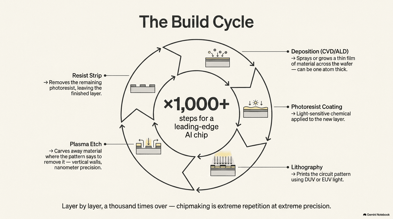
Think of it like sculpting, except you work in both directions. Sometimes you spray a new layer of material across the whole wafer (deposition). Sometimes you carve channels and holes into what's already there (etching). A modern chip is made by repeating this cycle — deposit, pattern with light, etch, deposit again — hundreds of times. A leading-edge AI chip can require more than a thousand individual processing steps, and a single wafer may pass through the lithography and etch tools dozens of times before it's finished.
Deposition: adding the layers
Deposition means laying down an ultra-thin film of material — metal, insulator, or semiconductor — across the wafer. These films can be just a few atoms thick, and they have to be perfectly uniform across a surface the size of a dinner plate.
There are several ways to do it. In chemical vapor deposition (CVD), gases flow over the heated wafer and react to leave a solid film behind. In atomic layer deposition (ALD), the film is built up literally one atomic layer at a time — the slowest but most precise method, used where thickness must be controlled to within a single atom. There's also epitaxy (growing a crystal layer that continues the wafer's own crystal structure) and electroplating (depositing copper wiring using an electric current in a chemical bath).
Two companies dominate this equipment. Applied Materials (AMAT) is the largest maker of chip-manufacturing equipment in the world, with a broad portfolio spanning deposition (ALD, CVD, epitaxy), the polishing step (CMP), ion implantation (shooting charged atoms into the silicon to change its electrical properties — the step that gives transistors the ability to switch on and off), and more. In its most recent quarter it reported record revenue of $7.91 billion and its highest gross margin in over 25 years. Lam Research (LRCX) is the other giant, with deep strength in both deposition and etch — its ALTUS, VECTOR, and Striker tools lay down the metal and insulator films, and management calls its Striker ALD the "tool of record at all leading memory makers" for a critical step in advanced DRAM (dynamic random-access memory — the fast, volatile memory chips that computers use as their working scratchpad) production (the same kind of memory that gets stacked into high-bandwidth memory).
Etching: carving it away
Etching is the reverse: removing material to leave behind the pattern that lithography defined. The photoresist (the light-hardened stencil from section 1.4) protects the areas you want to keep, and the etch tool eats away everything exposed.
Modern etching is done with plasma — an electrically charged gas that can carve features straight down with astonishing precision, digging trenches many times deeper than they are wide, with near-vertical walls. Getting a hole that deep and that narrow, without it bending or closing up, is one of the hardest tricks in manufacturing — and it gets harder every generation as the features shrink and the stacks (in memory chips especially) grow taller.
Lam Research leads here too, with its Kiyo, Flex, Vantex, and Aqara etch tools; Applied Materials competes with its Sym3 platform. This is a genuine two-horse race — the two companies are each other's primary competitor in both deposition and etch, alongside Japan's Tokyo Electron.
Why this matters for AI chips
Two shifts in chip design are pouring money into these tools. The first is a new transistor shape called gate-all-around (more on this in section 1.9), which requires many more deposition and etch steps than the previous design. Lam estimates that every 100,000 wafers per month of gate-all-around capacity adds roughly $1 billion to the market it can sell into. The second is high-bandwidth memory — the special stacked memory that sits next to AI chips, covered in Chapter 2 — which demands its own intensive deposition and etch steps. Both trends mean more passes through more machines, which is why Applied Materials and Lam Research have both been raising their growth outlooks.
The Cleanroom — Ultra-Pure Chemistry
Everything described so far — printing, depositing, etching — happens inside a room unlike any other on Earth: the cleanroom. The reason is simple and unforgiving. On a chip where the smallest features are a few nanometers across, a single speck of dust is a boulder. One stray particle landing on the wafer at the wrong moment can short a transistor and kill the chip. So the air in a fab is filtered until it is thousands of times cleaner than a hospital operating room, and the people inside wear head-to-toe "bunny suits" — not to protect themselves, but to protect the wafer from them. A human body sheds tens of thousands of particles a minute.
But clean air is only half of it. Every one of the hundreds of processing steps uses chemicals and gases, and each one has to be almost impossibly pure — because the same stray atom that ruins a transistor can arrive dissolved in a liquid or floating in a gas.
The gases
A working fab runs on a constant supply of gases piped in from tanks and on-site plants: nitrogen and argon to create inert, oxygen-free environments; hydrogen and oxygen for reactions; helium to cool wafers and carry heat away during lithography; and dozens of exotic "specialty gases" for specific etch and deposition steps. These come from the world's industrial-gas giants. Linde (LIN) is the largest industrial-gas company in the world, and its electronics business — the ultra-pure gases that feed advanced fabs — is its fastest-growing end market, which management attributes directly to AI-chip investment. Air Products (APD) is the other major supplier, often building and operating a gas plant right next to a fab; its high-purity helium business, critical for wafer cooling and lithography, rises and falls with semiconductor spending.
The liquids and the purity company
Between many steps the wafer is washed, coated, or polished, and each of those uses ultra-pure liquid chemistry — acids to etch, solvents to clean, and CMP slurries (the fine abrasive suspensions that polish each layer flat, first met in section 1.3). The company at the heart of keeping all of this clean is Entegris (ENTG). Entegris doesn't make chips — it makes the purity: the filters that strain contaminants out of the chemicals, the specialty deposition and etch materials, the CMP slurries and pads, and the sealed pods (called FOUPs) that carry wafers between machines without ever exposing them to open air. Without its filters and materials, yields crash and contaminated wafers become unsaleable.
Water gets the same treatment. A fab uses enormous volumes of "ultrapure water" to rinse wafers between steps — water so clean it would actually leach minerals out of your body if you drank it. DuPont (DD) supplies the ion-exchange resins that strip the last impurities out of that water, a business it ties directly to the data-center buildout.
The theme worth holding onto: chipmaking is as much a chemistry problem as an engineering one, and the companies that guarantee purity are a quiet but essential layer of the chain. We'll meet the raw materials these chemicals are made from — and where they come from — in Chapter 10.
The Number That Matters — Testing and Yield
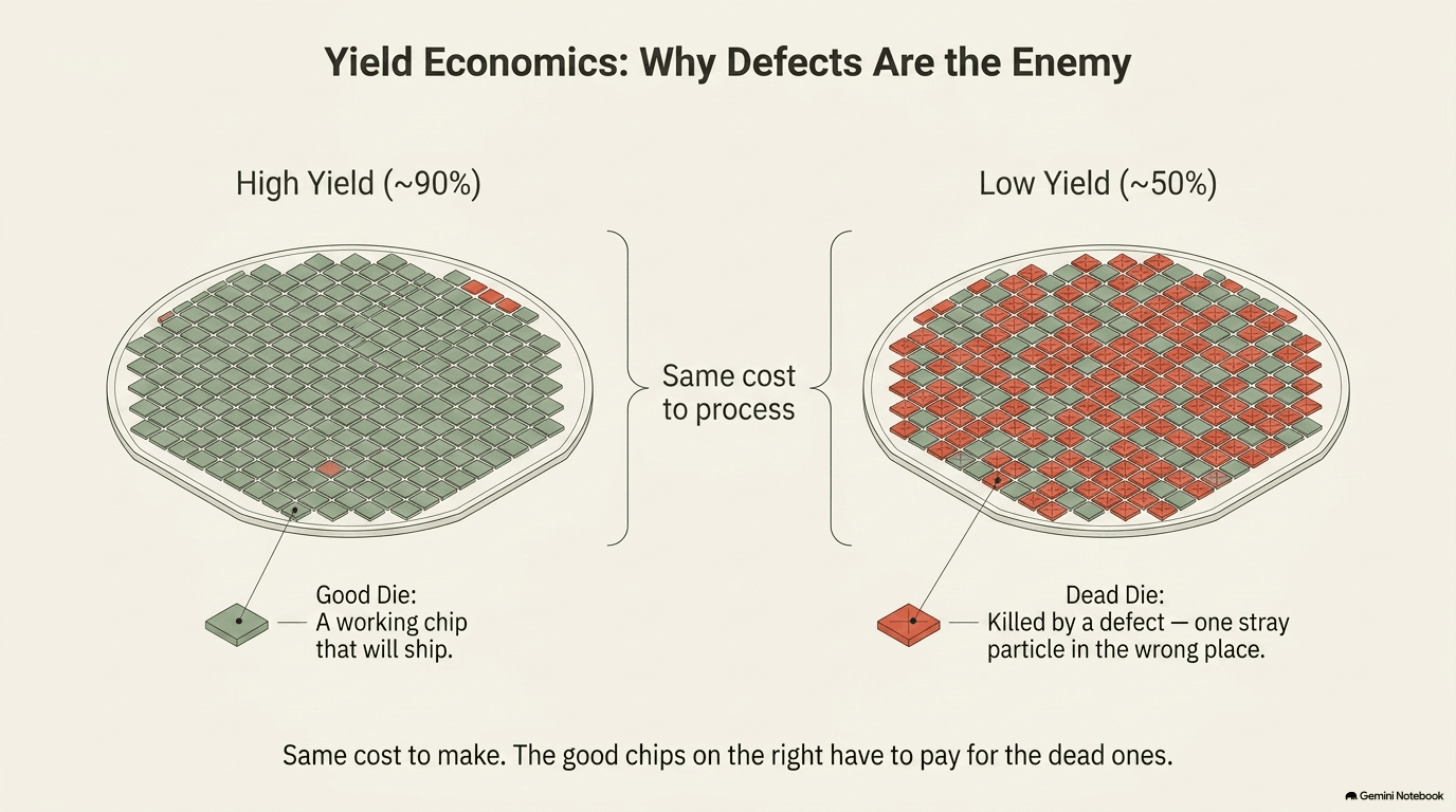
Here is a fact that surprises most people: when a chip factory makes a batch of chips, a meaningful fraction of them don't work. Some come out perfect. Some are dead. The percentage that come out good is called yield, and it is the single most important number in the entire industry.
Yield is why chipmaking is so brutally difficult, and so profitable when done right. A wafer costs roughly the same to process whether 90% of its chips work or 50% do. If yields are high, the good chips are cheap. If yields are low, every working chip has to carry the cost of its dead neighbors. A new manufacturing process often starts with painfully low yields and slowly climbs as engineers hunt down the sources of defects — a stray particle, a slightly misaligned layer, a contaminated chemical. For a chip with tens of billions of transistors, a single defect in the wrong place can kill the whole die — "die" being the industry's word for one individual chip on the wafer, before it's cut out and packaged.
So the industry spends enormous effort looking for defects — before, during, and after manufacturing. This splits into two jobs.
Finding defects on the wafer: process control
While the chip is still being built, engineers need to catch problems as early as possible — a defect caught after another 200 processing steps is 200 steps' worth of wasted work. This is the job of process control: inspection tools that scan the wafer for particles and pattern flaws, and metrology tools that measure whether each layer is the right thickness and properly lined up.
KLA (KLAC) dominates this niche almost the way ASML dominates lithography. It is the leading supplier of inspection and measurement equipment, with over half its revenue coming from wafer inspection alone. Its machines use everything from broadband light to focused beams of electrons to spot flaws far too small to see any other way. Process control has become even more critical for AI: high-bandwidth memory has "near-zero-defect requirements," in KLA's words, pushing the inspection intensity of memory chips up toward the levels once reserved for the most advanced logic.
Alongside the hardware sits a software layer. PDF Solutions (PDFS) provides big-data analytics — its Exensio platform gathers data from across the manufacturing line to help chipmakers find the patterns behind yield problems. As chips get more complex, squeezing out yield increasingly depends on this kind of data analysis, not just better microscopes.
Testing the finished chip: automated test
Once a chip is built and cut from the wafer, it has to be tested to confirm it actually works — every function, at speed, under real conditions. This is done by automated test equipment (ATE): machines that connect to each chip and run millions of checks in seconds.
Teradyne (TER) is a leader here. Its test systems check the AI accelerators, custom hyperscaler chips (such as Google's TPU and Amazon's Trainium), networking silicon, and memory that go into data centers. The company has been transformed by the AI wave — roughly 70% of its recent revenue is AI-related, up from around 40-50% about six months earlier — and its semiconductor-test business crossed $1 billion in a single quarter for the first time. It is also moving into testing the optical components (co-packaged optics) that Chapter 5 will cover.
Who Makes the Chip
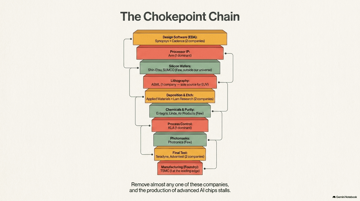
Step back, and a striking pattern emerges: at almost every stage of making a chip, the critical tools come from just one or two companies. This isn't a normal industry with dozens of interchangeable suppliers. It's a chain of chokepoints.
Here is the whole front end — designing and manufacturing the bare chip — in one map:
| Step | What happens | Who makes the tools | |---|---|---| | Design software (EDA) | The chip is designed in software | Synopsys, Cadence (duopoly) | | Processor IP | Pre-built core designs are licensed in | Arm (CPU cores); CEVA (connectivity, sensing, AI IP) | | Silicon wafers | Sand purified and grown into crystal disks | Shin-Etsu, SUMCO (mostly outside our universe) | | Lithography | The pattern is printed with light | ASML (sole source for EUV) | | Deposition & etch | Layers added and carved, ×1,000+ | Applied Materials, Lam Research | | Chemicals, gases & purity | Ultra-pure inputs, filtration, wafer handling | Entegris, Linde, Air Products, DuPont | | Process control | Wafers inspected and measured for defects | KLA (dominant); PDF Solutions (analytics) | | Photomasks & resist | Stencils and light-sensitive chemistry | Photronics; JSR, TOK, Shin-Etsu (Japanese) | | Final test | Finished chips checked at speed | Teradyne, Advantest | | Manufacturing (foundry) | All of the above, run at scale | TSMC (leading edge), Samsung, Intel |
The company that ties it all together is the foundry — the factory that owns the machines, runs the process, and turns a design file into physical chips. The dominant leading-edge foundry is TSMC of Taiwan; Samsung and Intel are the other two players attempting the most advanced nodes. A foundry doesn't make most of its own equipment — it buys the lithography from ASML, the deposition and etch from Applied Materials and Lam, the inspection from KLA — and combines them into a working production line. That makes the foundry both the customer every equipment company depends on, and the chokepoint every chip designer depends on.
We'll return to foundries — and to why so much of the world's most advanced manufacturing sits on a single island — when the buildout's geography comes up in later chapters. For now, the takeaway is the concentration itself: remove almost any one of these companies, and the production of advanced AI chips would stall.
What's Changing
The making of a chip is not a settled process. Three shifts are underway right now, and each one is reshaping which companies win.
The transistor is changing shape. For about a decade, the standard transistor design was called "FinFET" — the current-carrying channel stood up like a fin. That design is now running out of room. Its replacement is gate-all-around (GAA), in which the channel is wrapped on all four sides for better control at tiny scales. GAA is harder to build — it needs more deposition and etch steps, especially the atom-by-atom ALD process — which is exactly why the equipment makers are so optimistic. Applied Materials and Lam Research have both built new tool lines specifically for GAA, and both point to it as a major growth driver.
Power is moving to the back. On a normal chip, the wiring that carries data and the wiring that delivers power are stacked together on the front of the die, competing for space. A newer approach called backside power delivery moves the power wiring to the underside of the wafer, freeing the front for data and letting the chip run faster and more efficiently. Intel's 18A process — the same one using ASML's High-NA machines — is among the first to bring this to production. It adds yet more manufacturing steps.
The finest features need new light. As covered in section 1.4, High-NA EUV — ASML's next-generation lithography — has now entered real production at Intel, the first such use anywhere in the world. It will spread to other manufacturers and to memory over the next few years, gated as always by how fast Zeiss can build the optics.
And one shift points straight ahead to the next chapter. Making a single chip larger and larger is hitting physical limits — there's a maximum size a machine can print in one shot, and bigger chips have worse yields. So the industry is increasingly building systems out of several smaller chips — called chiplets — bonded tightly together into one package. That moves the action from the front end (making the die) to the back end (packaging), which is exactly where Chapter 2 begins.
Next: Chapter 2 — Packaging and Memory (from a single die to a working system)
Companies in this part of the buildout: Silicon Design, Chip Making