Chapter 9
The Factories
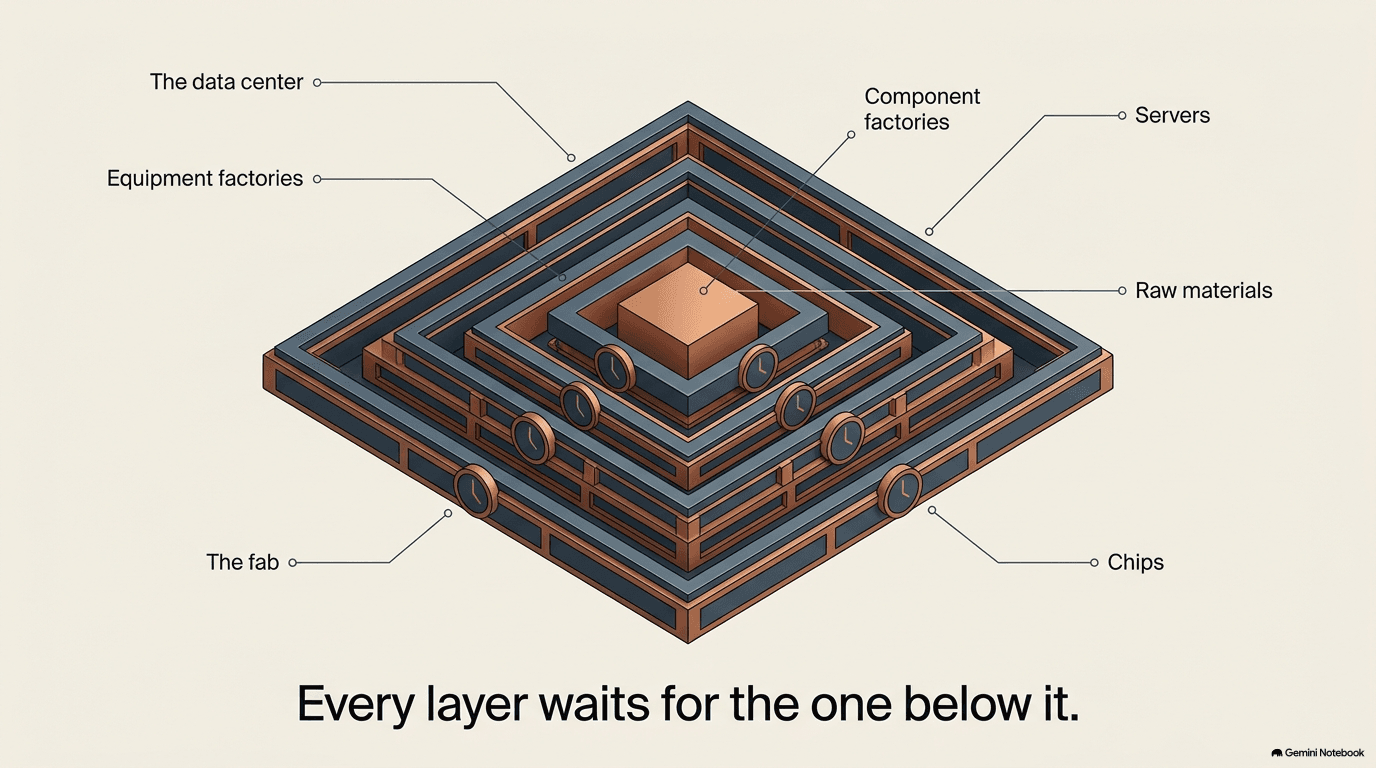
Every component described in the previous eight chapters was made in a factory somewhere, and at nearly every layer it is the factory's throughput — not the level of demand — that determines how fast AI infrastructure can actually grow.
This chapter turns the book inside out. Instead of asking "what does a data center need?" it asks "where does all that stuff come from?" The answer, almost everywhere, is: from a surprisingly small number of factories, most of which were already running flat out before AI arrived.
Why the Factory Is the Real Speed Limit
The previous eight chapters described what goes into an AI data center — chips, servers, networks, buildings, cooling systems, power equipment, turbines, grid connections, fiber. Each is essential. None can be left out. And here is the fact that matters most: almost every one of them is made in a factory that takes years to build, years to staff, and years to ramp to full speed. The factory, not the check, is the speed limit.
This creates a problem that money alone cannot solve. If demand doubles overnight — and in AI, something close to that actually happened — the supply chain cannot respond in kind. A semiconductor fab takes three to five years to build and another year or two to reach good yields. A transformer factory requires specialized steel mills, precision winding equipment, and workers whose skills take years to learn. A fiber-optic factory starts with a preform furnace that itself must be purpose-built. These are not assembly lines where you hire a second shift and double output by next quarter. They are capital-heavy, skill-heavy, physics-constrained facilities where the time between "we should build more" and "we are shipping more" is measured in years.
The result is a layered queue. The chip maker waits for the lithography machine. The lithography maker waits for the optics. The optics maker waits for the specialized glass. Each layer assumes the one below it can deliver — and when every layer is simultaneously capacity-constrained, the wait times don't just add; they compound. This chapter walks through the major factory types, from the most extreme (the semiconductor fab) to the most mundane (the logistics network), to show where the physical world pushes back.
The Semiconductor Fab
The factory that makes chips — called a fab, short for fabrication plant — is the single most expensive and complex factory humans build. A leading-edge fab costs somewhere between twenty and forty billion dollars, takes three to five years to construct, and another year or two to reach the yields (the fraction of chips that come out working) that make the economics viable. Why so expensive? Three reasons, each rooted in physics.
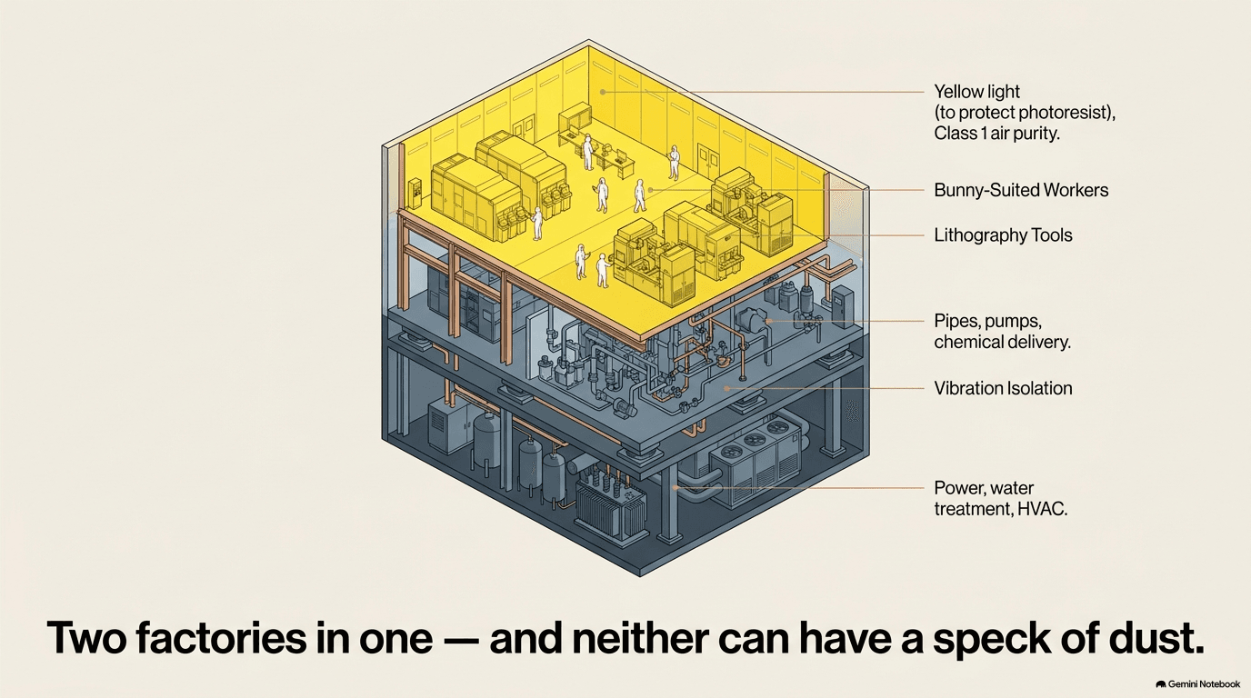
The cleanroom. The entire production floor is a cleanroom — a sealed environment where the air is filtered continuously so that the number of particles larger than half a micron per cubic foot stays close to zero. For context, a hospital operating room allows about ten thousand particles per cubic foot; a leading-edge fab allows fewer than one. A single speck of dust landing on a wafer during lithography can ruin a chip, because the features being printed are smaller than the dust particle itself. To maintain this, the air in the fab is replaced hundreds of times per hour by massive filtration systems, and every person inside wears a full-body "bunny suit" — head cover, face mask, gloves, booties — not to protect themselves from the chemicals, but to protect the wafers from them. Even the light is yellow: the photoresist chemicals used in patterning are sensitive to shorter wavelengths, so the fab is lit by filtered light that won't trigger them prematurely.
The sub-fab. Beneath the production floor is an entire second factory — the sub-fab — that most visitors never see, and whose complexity rivals the cleanroom itself.
The chemical delivery system is a network of ultra-pure piping that carries dozens of different gases and liquids to each tool. Some of these chemicals are merely exotic — ultra-high-purity nitrogen, argon, hydrogen. Others are genuinely dangerous: arsine and phosphine (used in doping) are lethal at concentrations measured in parts per million; silane (used in deposition) ignites spontaneously in air; hydrofluoric acid (used in etching) penetrates skin and attacks bone. Each chemical has its own dedicated piping system (you never want two reactive chemicals sharing a line), its own monitoring for leaks, and its own emergency-response protocol. The piping itself must be made of materials that won't contaminate the chemicals — electropolished stainless steel or specialized fluoropolymers — because a few parts per billion of metal contamination from the pipe walls can ruin a batch of wafers.
The vacuum systems serve the many tools that operate at pressures far below atmospheric — deposition tools, etch tools, and ion implanters all require vacuum chambers that can be pumped down to a billionth of atmospheric pressure. This requires banks of vacuum pumps — turbomolecular pumps, cryogenic pumps, dry pumps — running continuously. The exhaust from these pumps contains the process gases and must be treated before release.
The waste treatment systems handle the byproducts of all those chemical processes. Acidic rinse water is neutralized. Solvent waste is collected for specialized disposal. Exhaust gases are scrubbed, burned in thermal abatement systems, or treated with chemical neutralizers. A leading-edge fab consumes and treats millions of gallons of ultra-pure water per day — the water must be purified to parts-per-trillion levels before use and treated before discharge.
The vibration-isolation systems are among the most demanding in any industrial facility. The floor of the cleanroom must be isolated from traffic, wind, seismic activity, and even the vibrations of the fab's own pumps and fans, because the lithography systems are sensitive to vibrations of a few nanometers — far smaller than anything a human can feel. This typically means the cleanroom floor sits on massive concrete pads, separated from the rest of the building by isolation joints, with active damping systems that sense vibrations and generate counter-vibrations to cancel them out.
The sub-fab can be as large as the cleanroom above it — and in some fabs, it is larger.
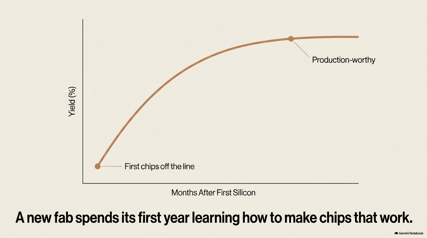
Yield. A new fab doesn't start by making good chips. It starts by making mostly bad ones. The first wafers through a new process might yield ten or twenty percent usable chips — the rest have defects. Over months of relentless debugging — adjusting temperatures, pressures, exposure doses, etch times — the yield climbs. A mature process might reach eighty or ninety percent. This ramp is the reason a fab takes years to become profitable: you are spending billions on construction and equipment while producing chips that mostly go in the trash, and only gradually does the ratio flip. Every contamination source must be found and eliminated: a slightly impure gas line, a worn part on an etch tool, a vibration that appears only when a compressor cycles on.
The wafer's journey. A single wafer spends two to four months inside the fab, passing through hundreds of individual process steps — often more than a thousand for a leading-edge chip. It is coated with photoresist, exposed to light through a mask, developed, etched, stripped, cleaned, deposited with a new layer of material, and the cycle repeats. Each layer of the chip requires multiple passes through the sequence, and a finished chip might have seventy or more layers stacked on top of each other, each one aligned to the ones below it with accuracy better than a nanometer. The wafer travels between tools on automated overhead transport systems — robotic vehicles running on ceiling tracks — because human hands would contaminate the surface. At regular intervals, the wafer is inspected by electron-beam or laser-scanning tools that check for defects invisible to any optical microscope. A wafer that fails inspection at step 400 has wasted the value of all 399 preceding steps, which is why yield engineering is so relentless.
The tools inside the fab are themselves staggeringly expensive and precise. A deposition tool lays down thin films of material — sometimes a single atomic layer at a time — using chemical gases, plasma, or physical sputtering. An etch tool removes material selectively, carving the patterns defined by the lithography step into the deposited film. A CMP (chemical-mechanical planarization) tool polishes each layer flat so the next one can be built on a level surface — imagine sanding a table between coats of lacquer, but at atomic scale. An ion implantation tool fires charged atoms into the silicon to create the doped regions that give transistors their electrical properties. Each of these tools costs tens of millions of dollars, requires regular maintenance and consumable replacement, and can process only a limited number of wafers per hour. A fab might contain several hundred such tools.
Water is worth a special mention. A leading-edge fab uses millions of gallons of ultra-pure water every day — water so clean that it contains fewer than five parts per billion of dissolved solids (tap water might contain 200-500 parts per million, roughly a hundred thousand times more). This water is used to rinse wafers between process steps, to dilute chemicals, and to feed the cooling systems. Producing it requires a dedicated water-purification plant within the fab campus: raw water passes through filters, reverse-osmosis membranes, ion-exchange columns, UV sterilizers, and final polishing stages until every detectable contaminant has been removed. The wastewater from the fab — now carrying trace amounts of the process chemicals — must be treated before discharge. A fab's water budget can rival that of a small city, and in water-stressed regions, securing the rights to that much water is a significant obstacle.
Power consumption is equally enormous. A leading-edge fab can draw 100-200 megawatts of continuous power — comparable to a small city or a large data center. The tools, the air-handling systems, the vacuum pumps, the chemical-delivery systems, and the lighting all contribute. A fab needs its own substation and often a dedicated feed from the high-voltage grid. The reliability of that power feed is critical: a momentary interruption can destroy an entire batch of wafers in mid-process, because many process steps (deposition, lithography) require continuous, stable conditions. This is why fabs invest heavily in backup power and power-quality systems — the same UPS and generator systems described in Chapter 6, but scaled for industrial loads.
The companies that operate fabs are few. TSMC (TSM) is the dominant contract manufacturer, running dozens of fabs across several countries. Intel (INTC) operates its own fabs and is working to open them to outside customers as a foundry. GlobalFoundries (GFS) and UMC (UMC) manufacture at less extreme feature sizes, serving the enormous market for chips that don't need to be at the bleeding edge — the power-management chips, the network interface controllers, the analog components that surround every AI GPU. Samsung operates its own foundry division. That is essentially the list — worldwide, the number of organizations capable of manufacturing leading-edge logic chips can be counted on one hand, and the majority of the world's most advanced production happens on a single island.
The Machine That Makes the Machine
A fab doesn't build its own tools. It buys them — the lithography systems, the deposition chambers, the etch tools, the inspection stations — from a separate tier of manufacturers, each of which operates its own specialized factory. These equipment makers are, in a real sense, the factory behind the factory.
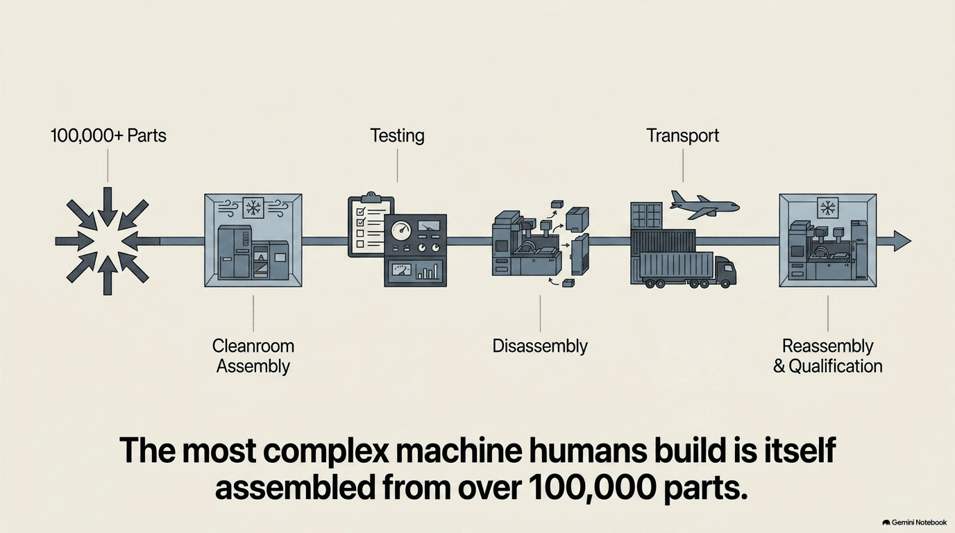
The most extraordinary case is the company that makes EUV lithography machines. ASML (ASML) is the sole manufacturer. Each system weighs roughly 180 tons, ships in dozens of containers, and takes many months to assemble. The assembly process itself happens in a cleanroom — because the optics inside the machine must be as flawless as the chips it will eventually help print. A single EUV system contains over 100,000 parts sourced from hundreds of suppliers across dozens of countries. The mirrors that focus the extreme-ultraviolet light are the smoothest large surfaces humans have ever made, polished to an accuracy of less than an atom, and they come from a single optics supplier — Carl Zeiss — whose production capacity directly limits how many machines can be built per year. This is the recursive structure at its most extreme: the factory that makes the chips depends on a machine that is itself one of the most complex things ever manufactured, and that machine depends on optics that only one company in the world can make.
The other equipment makers face similar, if less dramatic, constraints. Applied Materials (AMAT) and Lam Research (LRCX) build the deposition and etch tools — the workhorses of the fab, performing the hundreds of layering and carving steps each wafer goes through. A deposition tool must maintain a vacuum down to billionths of atmospheric pressure while delivering precisely metered flows of exotic gases — some of them toxic, some pyrophoric (they ignite on contact with air) — and striking a plasma that deposits atoms one layer at a time on a spinning wafer. An etch tool must carve trenches only a few nanometers wide into a surface, removing exactly the right material and stopping on a layer one atom thick, without damaging the layers above or below. Each tool is a precision vacuum chamber with dozens of gas lines, RF power supplies (which generate the radio-frequency energy that sustains the plasma), temperature controls, and endpoint-detection systems (sensors that monitor the chemical byproducts of the etching to detect the exact moment the etch has cut through the intended layer and is about to reach the layer below — telling the tool when to stop), assembled and tested over weeks. These companies have roughly doubled their own manufacturing capacity in recent years and are still working to keep pace with demand.
KLA (KLAC) makes the inspection and metrology tools — machines that use electron beams and laser scattering to find defects smaller than a virus. The challenge here is subtle: as chip features shrink, the defects that matter also shrink, and the inspection tools must keep up. A defect that would have been harmless at the 28-nanometer process node — a small bump, a slight contamination — becomes a killer at 3 nanometers because it's now a significant fraction of the feature size. So each new process generation demands not just smaller lithography but more sensitive inspection, and KLA's instruments must evolve in lockstep with the fab they serve.
The lead time from "order placed" to "tool installed and qualified in the customer's fab" is typically twelve to eighteen months, and longer for the most advanced lithography. During that time, the equipment maker must procure specialized components (many with their own months-long lead times), assemble the system, test it exhaustively, ship it (sometimes by dedicated cargo aircraft), and then spend weeks on-site installing and calibrating it. Only after all of that does the fab get a working tool — and a single fab might need dozens or hundreds of them.
The Server Factory
Compared to a semiconductor fab, a server factory looks almost conventional — it is an assembly line, not a cleanroom — but the scale and speed are extraordinary. The largest server and rack assemblers ship thousands of complete AI server racks per month, each one a multi-hundred-kilogram unit containing dozens of GPUs, hundreds of memory modules, custom cooling systems, and miles of internal cabling. The major contract manufacturers — Jabil (JBL), Flex (FLEX), Celestica (CLS) — and vertically integrated assemblers like Super Micro (SMCI) operate these lines.
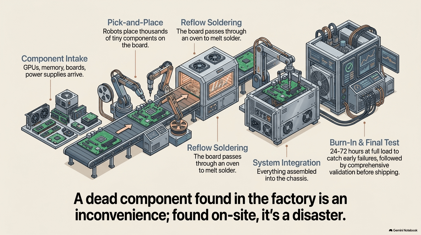
The assembly process has several stages. Component intake and inspection: GPUs, memory, network cards, power supplies, and chassis arrive from upstream suppliers and are checked against specifications. A single defective memory module in a 72-GPU server rack can be extraordinarily difficult to diagnose once the rack is powered up, so incoming quality control is strict. Board assembly: the printed circuit boards (motherboards, GPU carrier boards, network interface cards) are populated with components using automated pick-and-place machines and soldered in reflow ovens (conveyor-fed ovens that heat the entire board to a precise temperature profile, melting the solder paste that was deposited at each connection point and bonding every component to the board simultaneously) — the same process used in any electronics factory, but with unusually large, heavy, and expensive boards. System integration: the boards are installed in the chassis along with the cooling hardware, the power distribution, and the cabling, and the whole unit is connected and powered up for the first time.
Burn-in is the critical quality step, and its logic is worth understanding because it illustrates a general principle that appears throughout this book. Electronic components follow what reliability engineers call the bathtub curve: the failure rate is highest in the first few hours of operation (manufacturing defects that are just barely functional), drops to a low steady rate during the component's working life, and rises again near end of life (wear-out failures). The first hump — early failure, or "infant mortality" — is what burn-in targets.
Every completed server is run under full computational load — all GPUs active, maximum power draw, maximum heat — for an extended period, typically twenty-four to seventy-two hours. This is deliberately harsh: the factory is trying to break marginal components before the customer does. A GPU whose internal solder joint is slightly cracked will fail under sustained thermal cycling in the burn-in chamber; a memory module with a marginal cell will throw errors under sustained stress that it might pass in a quick power-on test. Finding and replacing a bad GPU in the factory is a minor inconvenience; finding it after the rack has been shipped, installed, cabled, and integrated into a customer's cluster is an expensive disaster that can delay the entire cluster's commissioning. Burn-in catches most of these before they leave the building.
The burn-in chambers themselves are substantial infrastructure: large, temperature-controlled rooms with heavy electrical feeds, dedicated cooling, and automated test harnesses that can run hundreds of systems simultaneously. They are one of the reasons server factories can't simply "add a shift and double output" — doubling production requires doubling the burn-in capacity, which requires more space, more power, and more cooling in the factory itself.
Automation is increasing rapidly. Machine-vision systems from companies like Cognex (CGNX) inspect solder joints and component placement at speeds no human could match. Industrial controllers from Rockwell Automation (ROK) and Emerson (EMR) manage the production lines. Robotic arms handle the heaviest components. Automated test systems run diagnostics without human intervention. The factory-automation companies are themselves a layer of the supply chain, and their order books reflect the same demand surge as everything else in this book.
The Power-Equipment Factory
If the semiconductor fab is the most complex factory in this story, the transformer factory may be the most constrained. Chapter 6 explained why transformers are essential — they step voltage up and down at every stage of the power chain — and why large ones are scarce. This section explains why they are so hard to make more of.
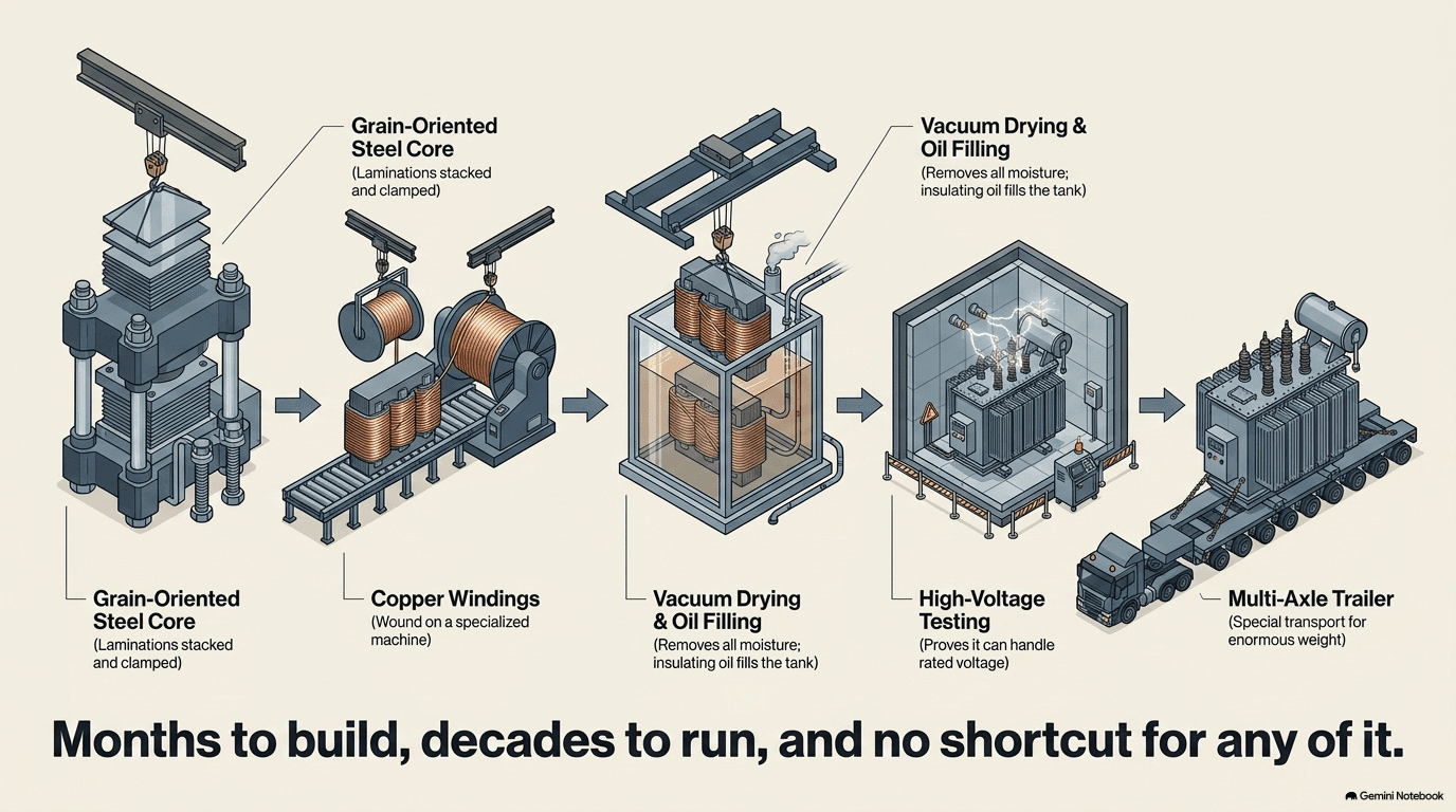
A large power transformer is a deceptively simple-looking object: a core of steel laminations wrapped with coils of copper or aluminum wire, sitting in a tank of insulating oil. But every aspect of that description hides difficulty.
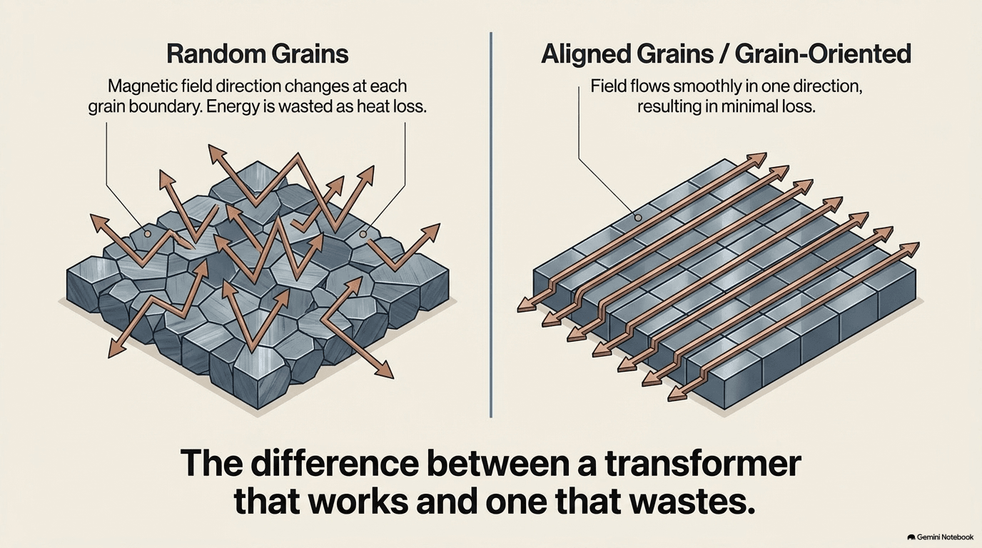
The core is made of grain-oriented electrical steel — a specialty alloy in which the crystal grains of the steel are aligned in one direction during manufacturing, so that the magnetic field passes through them with minimal energy loss. The "grain-oriented" part matters enormously: randomly oriented grains would waste far more energy as heat, and in a transformer handling tens of megawatts, even a few percentage points of loss represent enormous amounts of wasted power. This steel is made by a small number of mills worldwide, it requires a complex rolling and annealing process to achieve the grain alignment, and it has been in tight supply for years — anyone building a transformer factory must first secure a reliable source of this steel.
The windings are copper (or sometimes aluminum) wire, wound around the core in precise patterns that determine the transformer's voltage ratio and current capacity. In a large unit, the winding process is done on specialized machines by skilled technicians — there is no way to fully automate it, because each transformer design has different winding patterns, and the tolerances are tight. A winding error can cause a short circuit that destroys the transformer at first energization. The insulation between windings — layers of specially treated paper and pressboard, impregnated with oil — must withstand tens of thousands of volts without breakdown.
Testing is extensive. Every transformer is subjected to high-voltage tests (applying voltages well above its rated capacity to verify insulation integrity), impedance tests (measuring the transformer's internal electrical resistance to verify the windings are correctly assembled), temperature-rise tests (running it at full load and measuring how hot it gets), and sometimes partial-discharge tests (listening for tiny electrical sparks inside the insulation that would indicate a future failure). A transformer that passes all tests will typically operate for thirty to fifty years; one that fails testing may be unrepairable.
Assembly and filling take weeks: the core and windings are assembled, dried in a vacuum oven to remove all moisture from the insulation (moisture is the enemy of high-voltage insulation), lowered into the steel tank, and filled with highly refined mineral oil that both insulates and cools. The finished product can weigh hundreds of tons and must be transported on specialized multi-axle trailers, sometimes requiring road closures, bridge load assessments, and police escorts.
The result is a product that takes months to build, requires skilled labor that takes years to train, depends on specialty materials from a concentrated supply chain, and cannot be transported casually. This is why large power transformers have multi-year lead times, and why the sudden surge in data-center demand has created a bottleneck that money alone cannot quickly resolve. The major electrical-equipment manufacturers — Eaton (ETN), ABB (ABB), Powell (POWL) — are investing heavily in new factory capacity, but even a new transformer factory takes years to build and staff.
Switchgear and power-distribution equipment face similar, if less extreme, constraints. Medium-voltage switchgear — the circuit breakers and bus systems that distribute power inside a building (Chapter 6) — requires its own specialized manufacturing: precision metal fabrication, vacuum or gas-insulated interrupters, and extensive testing. The combination of demand from data centers, grid modernization, industrial electrification, and renewable-energy connections has stretched lead times across the board.
Glass, Copper, and the Last Mile
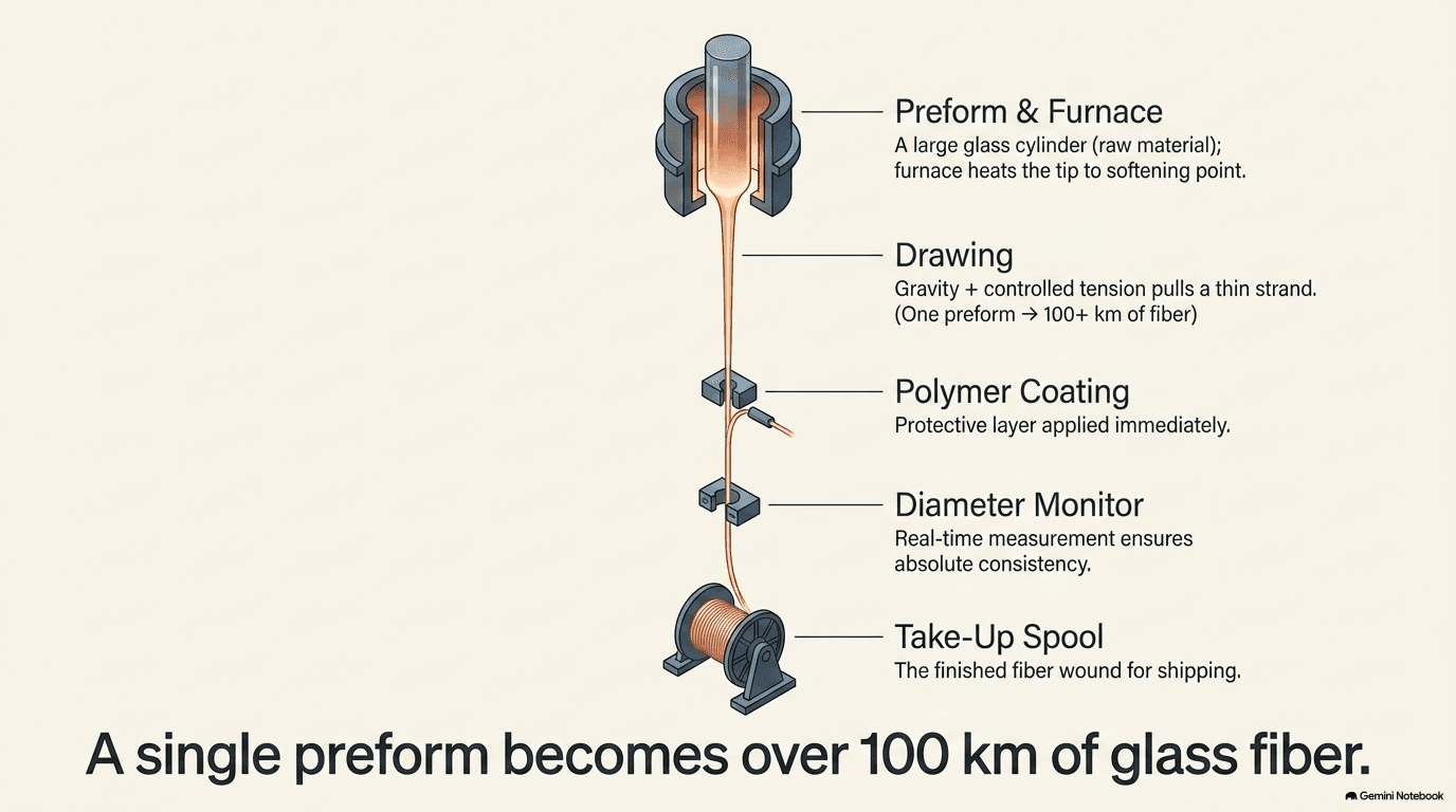
The fiber-optic cable from Chapter 3 starts its life as a cylinder of ultra-pure glass called a preform — typically about a meter long and ten centimeters in diameter. The preform is manufactured by depositing layers of glass with precisely controlled compositions (the core glass has a slightly higher refractive index than the cladding, which is what traps the light inside) using chemical vapor deposition. Making a good preform is the hard part — it determines the optical properties of every kilometer of fiber drawn from it.
The preform is then heated in a furnace until its tip softens, and a thin strand of glass — thinner than a human hair — is drawn out and pulled downward through a coating station that applies protective polymer layers. A single preform yields over a hundred kilometers of finished fiber. The drawing process runs continuously, the fiber descending through the coating cups at speeds that can exceed forty meters per second, and the diameter must be controlled to within a fraction of a micron over the entire length. Any variation in diameter disrupts the light transmission. Corning (GLW) is the dominant manufacturer, operating fiber-drawing factories across more than a dozen countries.
The fiber is then wound onto spools and tested — every kilometer is measured for attenuation (how much light is lost per unit length), bandwidth (how much data it can carry), and geometric accuracy (whether the core is truly centered within the cladding). Fiber that doesn't meet spec is scrapped. The good fiber is either shipped as bare fiber or assembled into cables — bundles of many fibers inside protective jackets designed for specific environments. An underground cable has an armored outer layer to resist damage from digging. An underwater cable has multiple layers of steel wire and waterproof jacketing. An indoor cable is designed for tight bends and flame resistance. An aerial cable is strung between poles and must resist wind, ice, and UV degradation. The same glass fiber goes into all of them, but the cable engineering around it is different for each application.
The connectors at each end of a fiber-optic cable are themselves precision components that deserve attention. The glass core of a standard single-mode fiber is only about nine microns in diameter — roughly one-tenth the width of a human hair. When two fibers are joined, their cores must be aligned to within a fraction of a micron, or the light won't couple efficiently across the junction and the signal is lost. This is achieved by polishing the fiber end to an optically flat surface, pressing it into a precision ceramic ferrule (a small cylinder that holds the fiber in place), and then mating the two ferrules in a spring-loaded adapter that pushes the two polished faces together. Amphenol (APH) is among the largest connector manufacturers, operating hundreds of facilities worldwide with increasing automation for the most demanding products. The connectors for high-density data-center applications — the MPO/MTP multi-fiber connectors that carry twelve or twenty-four fibers in a single plug — require even tighter alignment across every fiber in the array, and their manufacturing is a precision-optics exercise disguised as a cable accessory.
Copper cable — power cables, building wire, data cables — involves a different but equally scaled process. Copper cathode (refined from ore, 99.99% pure — see Chapter 10) arrives at the wire mill as thick plates, which are melted and cast into long rods. The rods are drawn through progressively smaller dies — hardened steel or diamond — until the wire reaches the desired diameter, which can range from several millimeters for heavy power cable down to fractions of a millimeter for fine electronics wire. Between drawing stages, the wire is annealed (heated and cooled) to restore its ductility, because the drawing process work-hardens the metal and makes it brittle. The finished wire is then insulated (with PVC, cross-linked polyethylene, or other materials depending on the voltage and application), stranded (multiple wires twisted together for flexibility), jacketed (enclosed in an outer protective layer), and wound onto reels.
The variety is staggering. A single data center requires dozens of different cable types: heavy-gauge power cables rated for thousands of volts, medium-voltage feeder cables, branch circuit wire, control cables for the building-management system, Cat6A or Cat8 Ethernet cables (categories of copper data cable rated for progressively higher speeds) for management networks, grounding conductors, fire-alarm wire, and speaker cable for the emergency notification system. Each has its own specifications, its own insulation rating, its own test requirements. A single large data center uses millions of pounds of copper cable, and the cable factories are running at capacity across all product lines simultaneously.
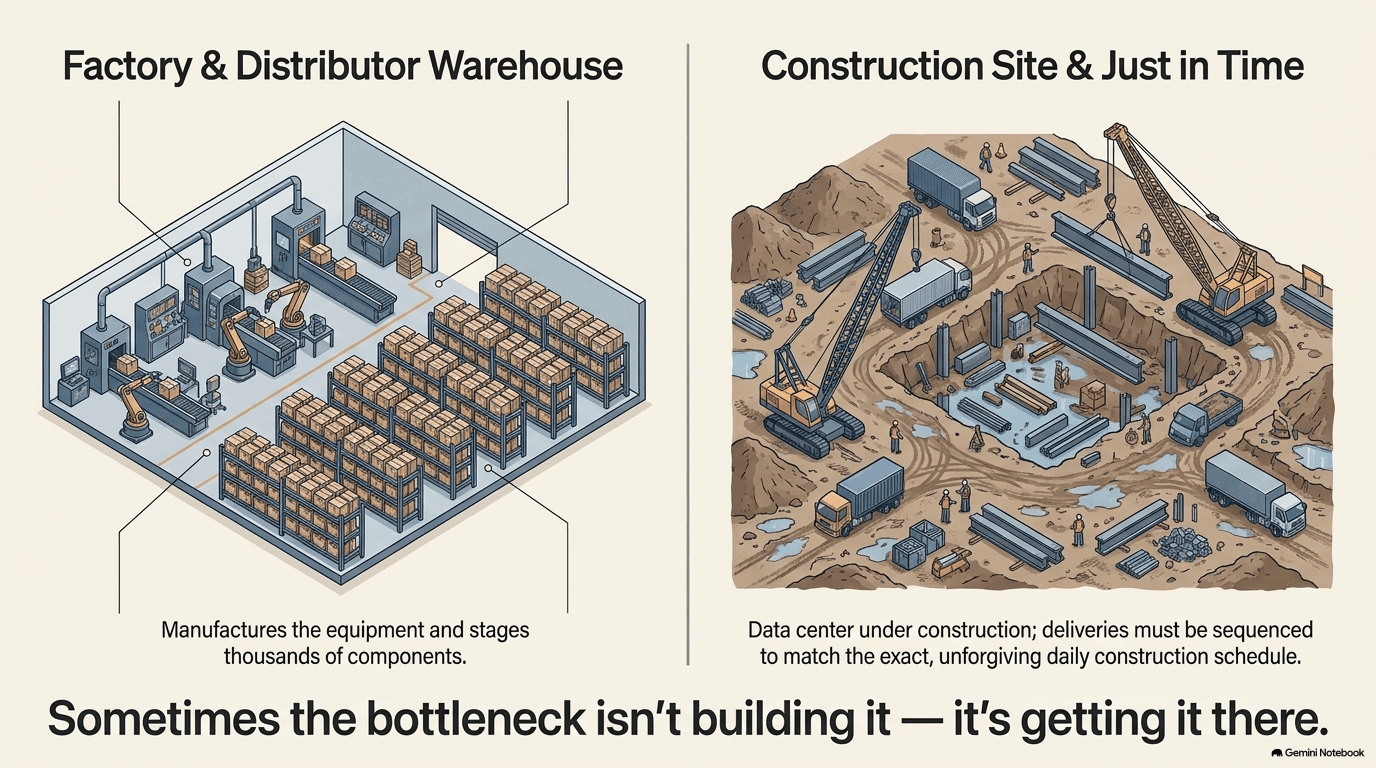
Distribution and logistics are the last and often most underestimated bottleneck. A data center under construction doesn't buy from hundreds of separate vendors — it buys through distributors who stock the thousands of electrical, mechanical, and electronic components a build requires. These distributors — companies like WESCO (WCC) and Applied Industrial (AIT) — operate massive warehouses and maintain relationships across the supply chain, providing a single point of contact for everything from copper bus bars to fire-suppression nozzles.
The physical transportation of the largest components deserves its own attention, because it reveals constraints that don't appear in any engineer's specification sheet. A multi-hundred-ton power transformer cannot simply be loaded onto a truck. It must travel on a heavy-haul trailer — a custom vehicle with dozens of axles spread over many meters to distribute the weight below bridge load limits. The route must be surveyed in advance: every overpass must be checked for vertical clearance, every bridge for load rating, every turn for the trailer's turning radius (which can exceed that of most intersections). Some routes require utility lines to be temporarily raised or removed. Police escorts are standard; in some jurisdictions, the move can only happen at night, on specific days of the week, to minimize traffic disruption. A move that covers a hundred miles may take several nights and cost hundreds of thousands of dollars in permits, escorts, and preparation.
A lithography machine (section 9.3) presents a different challenge: it travels in dozens of separate containers that must be climate-controlled and vibration-monitored throughout the journey. ASML ships the most advanced systems by dedicated cargo aircraft — the machines are too sensitive to survive the vibration and handling of ocean freight. A single 747 cargo flight from the Netherlands to Taiwan or Arizona carries one system's worth of containers, and the containers are fitted with sensors that record every shock and temperature excursion during transit. Any recorded event outside tolerance means the optics may have shifted, and the machine must be recalibrated (or in extreme cases, the affected components replaced) before installation can proceed.
Server racks present yet another logistical challenge: a fully assembled AI server rack weighs nearly a metric ton and is too fragile (densely populated circuit boards, liquid-cooling fittings, thousands of cable connections) to survive the jolts of long-distance trucking. Many assemblers therefore ship servers partially disassembled — boards packed separately from chassis, GPUs in anti-static cushioned crates — and perform final assembly and burn-in either at a staging facility near the data center or on site. This adds days to the installation timeline but avoids the expensive problem of components damaged in transit.
Sometimes the bottleneck isn't building the equipment at all; it's getting it to where it's needed, intact, on time, and in the right sequence — because a transformer that arrives before the pad it sits on is poured has nowhere to go, and a server rack that arrives after the cooling system's commissioning window has closed can't be tested.
Next: Chapter 10 — The Materials (what everything is made of, and where it comes from)
Companies in this part of the buildout: Chip Making, Servers & Compute, Power Systems